
Changjian Xie, Xihua Zou, Fang Zou, Yong Zhang, "High-performance ultra-compact polarization splitter-rotators based on dual-etching and tapered asymmetrical directional coupler," Chin. Opt. Lett. 19, 121301 (2021)
- Chinese Optics Letters
- Vol. 19, Issue 12, 121301 (2021)
Abstract
Keywords
1. Introduction
Photonic integrated circuits (PICs) fabricated in the silicon-on-insulator (SOI) platform are essential for massive applications in communications, military, and sensing. Due to its CMOS compatibility and ultra-high index contrast in the SOI platform, the PICs can be fabricated with low cost and compact footprint[
In this Letter, we design two novel PSRs, and one sample of them is fabricated by using electron-beam lithography (EBL). Both PSRs are dual etched in the through-port waveguide. The first level taper etching is used to meet the phase matching condition, for achieving the high-efficiency cross coupling between the
2. Design and Principle
The ultra-compact PSRs are designed based on the ADC structure. The top cladding of the PSR is specified as air to achieve a more compact footprint[
Sign up for Chinese Optics Letters TOC. Get the latest issue of Chinese Optics Letters delivered right to you!Sign up now
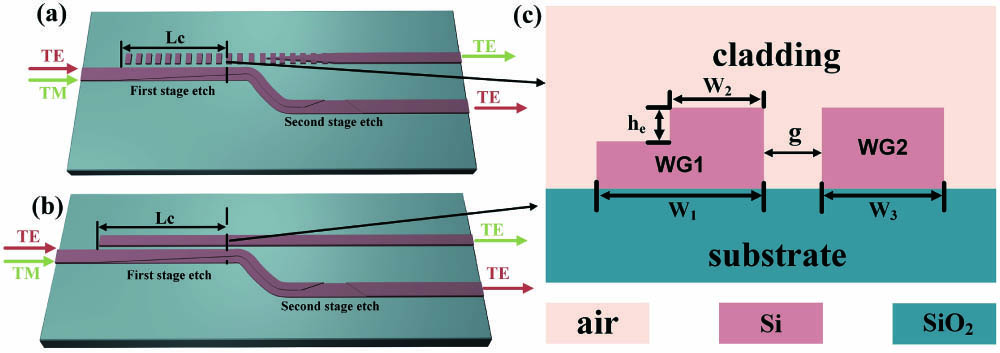
![]()
Figure 1.Schematic diagrams of the two proposed PSRs. (a) PSR-1. (b) PSR-2. (c) Cross view.
For the two PSRs,
![]()
Figure 2.Coupling efficiency of PSR-1 varies with the Lc.
For the nanowire waveguide in PSR-2,
![]()
Figure 3.Output powers from the through and cross ports vary with the length of Lc. (a) g = 100 nm, (b) g = 150 nm.
Figure 4 shows the conversion efficiency at the cross port and the through port of PSR-1 and PSR-2. Clearly, the ER is higher than 15 dB and 25 dB, and the loss is lower than 1 dB and 0.3 dB within the 130 nm and 20 nm bandwidth for PSR-1, respectively. For PSR-2, the obtained ER is higher than 15 dB, 20 dB, or 30 dB, while the loss is lower than 0.4 dB, 0.9 dB, or 1 dB within the bandwidth of 33 nm, 100 nm, or 150 nm, as shown in Figs. 4(c) and 4(d).
![]()
Figure 4.Conversion efficiency of PSR-1 at the (a) cross port and (b) through port; conversion efficiency of PSR-2 at the (c) cross port and (d) through port.
To reveal the fabrication tolerance of the two PSRs, we keep the center position constant and synchronously change the waveguide width. The results are shown in Fig. 5. PSR-1 and PSR-2 have
![]()
Figure 5.Fabrication tolerance of (a) PSR-1 and (b) PSR-2.
3. Fabrication and Measurement
Based on the above analysis, we fabricated the PSR-2 within a
![]()
Figure 6.(a) SEM images of the reference waveguide and PSR. (b) Main structure of the PSR.
We designed two vertical coupling gratings for supporting the
![]()
Figure 7.Transmission response of the (a) TE0 and (b) TM0 vertical coupling gratings.
The experiment and simulation results for PSRs are shown in Fig. 8, after being calibrated with the reference waveguide. The IL of the
![]()
Figure 8.Transmission spectral responses: (a) TM0 mode launched and (b) TE0 mode launched.
In addition, a comparison among similar PSRs recently reported is listed in Table 1. It is clear that the fabricated PSR-2 has excellent comprehensive characteristics in compact footprint, PCL, ER, and bandwidth, particularly the highest ER of 28 dB within the 45 nm bandwidth.
| Structure | Footprint (µm) | PCL (dB) | ER (dB) | Bandwidth (nm) | Tolerance (nm) |
|---|---|---|---|---|---|
| Sub-wavelength grating coupler and secondary filtering[ | 13 | 73 | |||
| Sub-wavelength grating coupler[ | 35 | 0.3 | 10 | 50 | |
| Discretized subwavelength nanostructure[ | 7.92 | 1 | 25 | 40 | |
| Counter-tapered coupler[ | 170 | 0.8 | 18 | 60 | |
| Mode-evolution and an asymmetric directional coupler[ | 170 | 1.5 | 10 | 40 | |
| This work | 28 | 1 | 28 | 45 |
Table 1. Performance Comparison among PSRs (Fabricated Samples)
4. Conclusion
We have designed two novel PSRs based on the dual-etched and tapered ADC. The
References
[1] X. Wang, G. Zhou, Z. Jin, L. Lu, G. Wu, L. Zhou, J. Chen. Wavelength-mode pulse interleaver on the silicon photonics platform. Chin. Opt. Lett., 18, 031301(2020).
[2] Y. Zhang, Y. He, X. Jiang, B. Liu, C. Qiu, Y. Su, R. A. Soref. Ultra-compact and highly efficient silicon polarization splitter and rotator. APL Photon., 1, 091304(2016).
[3] T. Tsuchizawa, K. Yamada, H. Fukuda, T. Watanabe, J.-I. Takahashi, M. Takahashi, T. Shoji, E. Tamechika, S. Itabashi, H. Morita. Microphotonics devices based on silicon microfabrication technology. IEEE J. Sel. Top. Quantum Electron., 11, 232(2005).
[4] W. Bogaerts, R. Baets, P. Dumon, V. Wiaux, S. Beckx, D. Taillaert, B. Luyssaert, J. V. Campenhout, P. Bienstman, D. V. Thourhout. Nanophotonic waveguides in silicon-on-insulator fabricated with CMOS technology. J. Lightwave Technol., 23, 401(2005).
[5] D. Dai, K. Ma, H. Wu. “Mode/polarization manipulation in silicon photonics. J. Phys. Conf. Series, 844, 012039(2017).
[6] S. Keyvaninia, H. Boerma, M. Wössner, F. Ganzer, P. Runge, M. Schell. Highly efficient passive InP polarization rotator-splitter. Opt. Express, 27, 25872(2019).
[7] J. Wang, B. Niu, Z. Sheng, A. Wu, W. Li, X. Wang, S. Zou, M. Qi, F. Gan. Novel ultra-broadband polarization splitter-rotator based on mode-evolution tapers and a mode-sorting asymmetric Y-junction. Opt. Express, 22, 13565(2014).
[8] H. Liang, R. Soref, J. Mu. Compact polarization splitter based on a silicon angled multimode interferometer structure. Appl. Opt., 58, 4070(2019).
[9] Y. Ding, H. Ou, C. Peucheret. Wideband polarization splitter and rotator with large fabrication tolerance and simple fabrication process. Opt. Lett., 38, 1227(2013).
[10] B. Bai, L. Pei, J. Zheng, T. Ning, J. Li. Ultra-short plasmonic polarization beam splitter-rotator using a bent directional coupler. Chin. Opt. Lett., 18, 041301(2020).
[11] Z. Ying, G. Wang, X. Zhang, H.-P. Ho, Y. Huang. Ultracompact and broadband polarization beam splitter based on polarization-dependent critical guiding condition. Opt. Lett., 40, 2134(2015).
[12] J. Wang, B. Niu, Z. Sheng, A. Wu, X. Wang, S. Zou, M. Qi, F. Gan. Design of a SiO2 top-cladding and compact polarization splitter-rotator based on a rib directional coupler. Opt. Express, 22, 4137(2014).
[13] L. Liu, Y. Ding, K. Yvind, J. M. Hvam. Silicon-on-insulator polarization splitting and rotating device for polarization diversity circuits. Opt. Express, 19, 12646(2011).
[14] Y. Xiong, J. G. Wangüemert-Pérez, D.-X. Xu, J. H. Schmid, P. Cheben, W. N. Ye. Polarization splitter and rotator with subwavelength grating for enhanced fabrication tolerance. Opt. Lett., 39, 6931(2014).
[15] B. Bai, L. Liu, Z. Zhou. Ultracompact, high extinction ratio polarization beam splitter-rotator based on hybrid plasmonic-dielectric directional coupling. Opt. Lett., 42, 4752(2017).
[16] Y. Xiong, D.-X. Xu, J. H. Schmid, P. Cheben, S. Janz, W. N. Ye. Fabrication tolerant and broadband polarization splitter and rotator based on a taper-etched directional coupler. Opt. Express, 22, 17458(2014).
[17] C. Xie, X. Zou, P. Li, L. Yan, W. Pan. Ultracompact silicon polarization splitter-rotator using a dual-etched and tapered coupler. Appl. Opt., 59, 9540(2020).
[18] Y. He, Y. Zhang, X. Wang, B. Liu, X. Jiang, C. Qiu, Y. Su, R. Soref. Silicon polarization splitter and rotator using a subwavelength grating based directional coupler. Optical Fiber Communication Conference, Th1G.6(2017).
[19] Y. Zhang, Y. He, H. Wang, L. Sun, Y. Su. Ultra-broadband mode size converter using on-chip metamaterial-based Luneburg lens. ACS Photon., 8, 202(2021).
[20] Y. Wang, M. Ma, H. Yun, Z. Lu, X. Wang, N. A. F. Jaeger, L. Chrostowski. Ultra-compact sub-wavelength grating polarization splitter-rotator for silicon-on-insulator platform. IEEE Photon. J., 8, 7805709(2016).
[21] Y. Liu, S. Wang, Y. Wang, W. Liu, H. Xie, Y. Yao, Q. Song, X. Zhang, Y. Yu, K. Xu. Subwavelength polarization splitter-rotator with ultra-compact footprint. Opt. Lett., 44, 4495(2019).
[22] K. Yu, L. Wang, W. Wu, Y. Luo, Y. Yu. Demonstration of an on-chip broadband polarization splitter and rotator using counter-tapered coupler. Opt. Commun., 431, 58(2019).
[23] C. Yuan, J. Dai, H. Jia, J. Ding, L. Zhang, X. Fu, L. Yang. Design of a C-band polarization rotator-splitter based on a mode-evolution structure and an asymmetric directional coupler. J. Semicond., 39, 124008(2018).


Set citation alerts for the article
Please enter your email address

© Copyright 2018-2021 | Chinese Laser Press. All Rights Reserved 沪ICP备15018463号-20