
Yi-Fei Geng, Zhu-Ning Wang, Yao-Guang Ma, Fei Gao. Topological surface plasmon polaritons [J]. Acta Physica Sinica, 2019, 68(22): 224101-1
- Acta Physica Sinica
- Vol. 68, Issue 22, 224101-1 (2019)
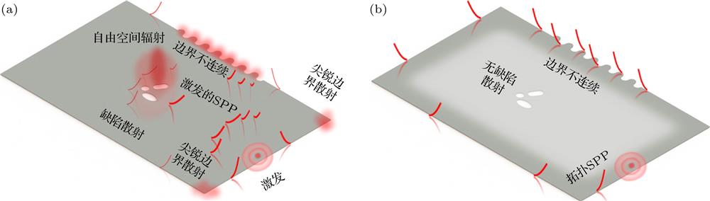
Fig. 1. (a) Effect of impurity and structural defects on surface plasmon transport; (b) robust propagation characteristics of topological surface plasmons.(a)杂质和结构缺陷对表面等离激元传输的影响; (b)拓扑表面等离激元的鲁棒传输特性
![Two-dimensional topological surface plasmon crystals and their boundary states [30]: (a) Schematic diagram of triangular circular hole lattices in graphene, under the action of an applied magnetic field B, finite lattices support a unidirectional edge plasma with topological protection; (b) energy band diagram of plasmon in graphene of B ≠ 0, when d ≠ 0, the complete band gap appears; (c) edge states under different magnetic induction and their robustness二维拓扑表面等离激元晶体及其边界态[30] (a)石墨烯中圆孔三角点阵的示意图, 在外加磁场B作用下, 有限晶格支持拓扑保护的单向边缘等离子体; (b)在B ≠ 0的石墨烯中的等离激元色散能带, 当孔径d ≠ 0, 出现完全带隙; (c)不同磁感应强度下的边界态及其鲁棒性](/richHtml/wlxb/2019/68/22/20191085/img_2.jpg)
Fig. 2. Two-dimensional topological surface plasmon crystals and their boundary states [30]: (a) Schematic diagram of triangular circular hole lattices in graphene, under the action of an applied magnetic field B , finite lattices support a unidirectional edge plasma with topological protection; (b) energy band diagram of plasmon in graphene of B ≠ 0, when d ≠ 0, the complete band gap appears; (c) edge states under different magnetic induction and their robustness
二维拓扑表面等离激元晶体及其边界态[30] (a)石墨烯中圆孔三角点阵的示意图, 在外加磁场B 作用下, 有限晶格支持拓扑保护的单向边缘等离子体; (b)在B ≠ 0的石墨烯中的等离激元色散能带, 当孔径d ≠ 0, 出现完全带隙; (c)不同磁感应强度下的边界态及其鲁棒性
Fig. 3. (a) Schematic diagram of graphene-based energy valley plasmon crystals: a gate structure with a biased voltage V 0 and an angle with respect to the graphene lattice; (b) energy band at the Dirac point; (c) electric field distribution on the yz (x = 0) plane; (d) two types of boundaries; (e) valley chern numbers corresponding to different angles; and (f) the one-dimensional structural energy band shown in Fig. (d).
(a)基于石墨烯的能谷等离子激元晶体示意图: 由偏置电压V 0与相对于石墨烯晶格存在夹角的栅结构; (b)狄拉克点处的能带; (c) yz (x = 0)平面上的电场分布; (d)两种类型的边界; (e)不同夹角对应的谷陈数值; (f)图(d)所示一维结构能带[32]
Fig. 4. Spoof plasmonic QSH[27,37]: (a) Photonic QSH with dielectric cylinders, the zoom in figure shows the hexagonal cluster; (b) edge states of photonic QSH; (c) spoof plasmonic structure whose unit cells of hexagonal clusters get shrunk, leading to zero spin Chern number; (d) spoof plasmonic structure whose unit cells of hexagonal clusters get expanded, which generates non vanishing spin Chern number; (e) simulated edge states at a domain wall between structures of (c) and (d); (f) constructed domain wall by combining structures in (c) and (d); (g) field patterns of edge states
人工表面等离激元QSH[27,37] (a)基于介质圆柱的光子QSH阵列; (b)图(a)中结构的能带; (c)单元胞收缩的SSPPs结构; (d)单元胞扩张的SSPPs结构; (e)SSPPs结构的能带仿真结果; (f)通过组合(c)和(d)中的结构构建边界; (g)边界态的模场分布
Fig. 5. Spoof plasmonic VHE and QVH[38,41,42]: (a) Schematic of TMDS; (b) band structure of TMDS in the first Brillouin zone; (c) spoof-SPP platform for VHE; (d) experimental demonstration of spoof-SPP VHE; (e) spoof-SPP platform for QVH; (f) experimental demonstration of spoof-SPP QVH
人工表面等离激元VHE和QVH[38,41,42] (a)二维过渡金属二硫化物(TMDS)的示意图; (b)第一布里渊区TMDS的能带结构; (c)用于VHE的SSPPs结构; (d) SSPPs-VHE的模场扫描结果; (e)用于QVH的SSPPs结构; (f) SSPPs-QVH的模场测试结果
Fig. 6. Spoof plasmonic demonstration of the anomalous Floquet topological phase[14]: (a) Photo of spoof plasmonic rings; (b) a 5 by 5 lattice inexperiment; (c) topological transition as the inter-ring coupling increases; (d) observed field pattern when the excitation is inside the bulk at frequency11.3 GHz; (e) observed edge state at frequency 11.3 GHz; (f) the edge state circumvents and tunnels through a defect lattice
基于SSPPs结构的反常Floquet拓扑相[14] (a)人工表面等离激元环的照片; (b)实验中5 × 5点阵; (c)随着环间耦合的增加产生的拓扑相变; (d)当激励源频率为11.3 GHz时在阵列内观察到的局域模场; (e)在11.3 GHz频率观察到的边界态; (f)边界态绕过缺陷晶格传播


Set citation alerts for the article
Please enter your email address

© Copyright 2018-2021 | Chinese Laser Press. All Rights Reserved 沪ICP备15018463号-20