
Muguang Wang, Yu Tang, Jian Sun, Jing Zhang, Qi Ding, Beilei Wu, Fengping Yan, "Photonic-assisted FSK signal generation based on carrier phase-shifted double sideband modulation," Chin. Opt. Lett. 19, 103901 (2021)
- Chinese Optics Letters
- Vol. 19, Issue 10, 103901 (2021)
Abstract
Keywords
1. Introduction
Traditionally, microwave signals generated in the electrical domain by electronic devices have limited bandwidth and tunability, owing to the electronic bottleneck. Having the intrinsic advantages of broadband, reconfigurability, low system complexity, and immunity to electromagnet interference, microwave photonics has attracted more and more research interests in radar systems[
A binary FSK signal is represented in terms of two frequencies. The frequency carrying bit ‘1’ is called the mark frequency, and the other frequency carrying bit ‘0’ is designated the space frequency. How to switch between the mark frequency and the space frequency is a key technique for FSK signal generation. Cao et al. reported an FSK signal generation scheme by switching the bias point of a Mach–Zehnder modulator (MZM)[
In this Letter, we propose and experimentally demonstrate a photonic-assisted approach for FSK signal generation based on specially designed carrier phase-shifted double sideband (CPS-DSB) modulation. The joint operation of the polarization-sensitive MZM and phase modulator (PM) helps to realize the switch between mark frequency and space frequency by introducing different phase shifts between the optical carrier (OC) and the
Sign up for Chinese Optics Letters TOC. Get the latest issue of Chinese Optics Letters delivered right to you!Sign up now
2. Principle
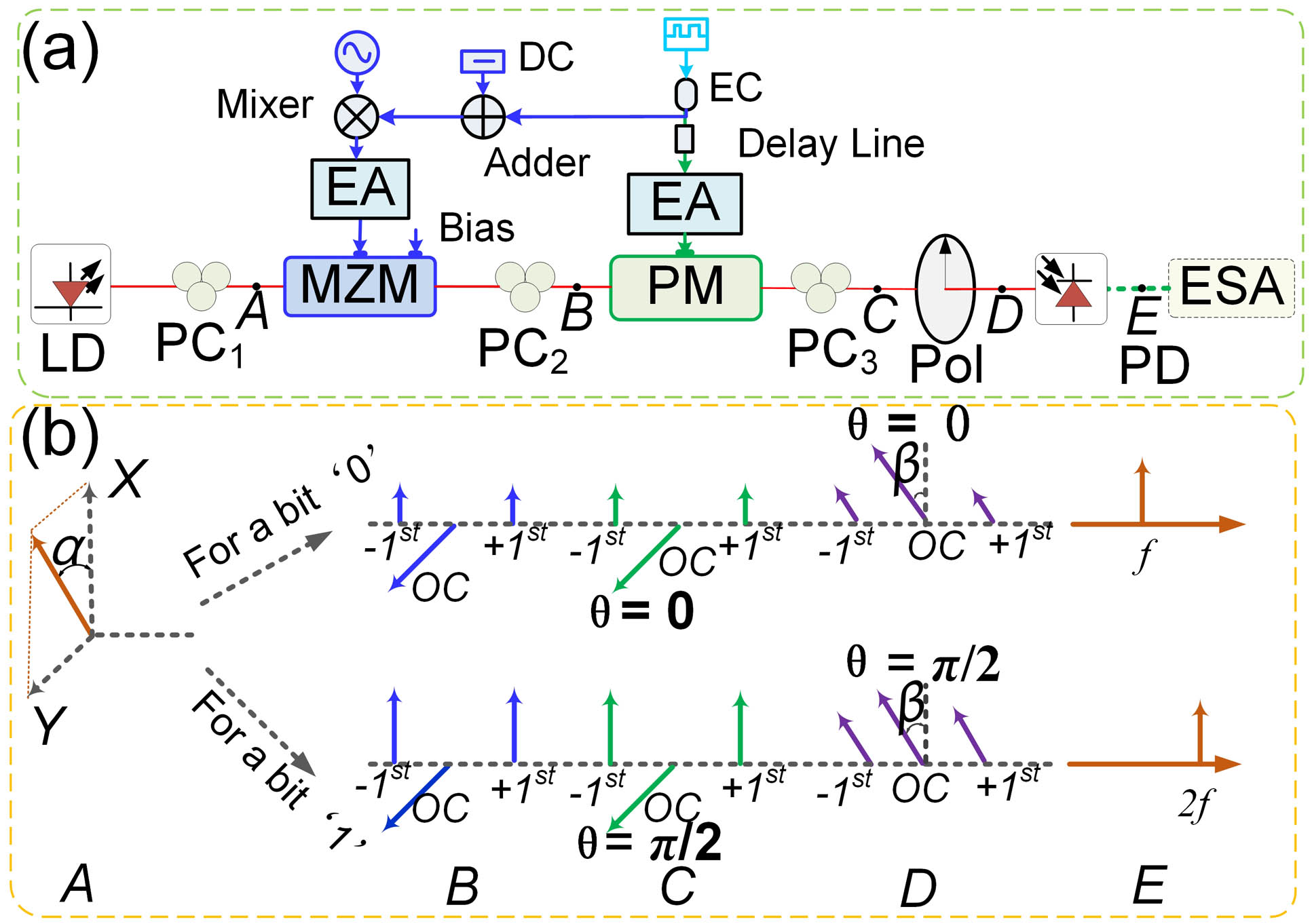
The proposed schematic diagram for FSK signal generation based on the photonic-assisted CPS-DSB technique is shown in Fig. 1(a), and the spectral evolution of the polarized light wave at different positions is also depicted in Fig. 1(b). The polarization direction of the linearly polarized continuous-wave (CW) light wave emitted from a laser diode (LD) is adjusted to have an angle of
![]()
Figure 1.(a) Proposed schematic diagram for FSK signal generation based on CPS-DSB modulation. (b) Spectral evolution of the injected CW light wave at different positions in the system.
When a microwave signal
Considering the small signal modulation condition and the bias point of the MZM, only the OC and the
Then, optical-to-electrical conversion is performed in the PD. Ignoring the DC component, the electrical current can be expressed as
To optimize the amplitude of the electrical current, let
Recall that
The above operation principle can also be explained by analyzing the relationship of the beat signals between different optical-frequency components of the modulated signal. As shown in Fig. 1(b) at position
For an FSK signal, the amplitude of the mark-frequency signal and the space-frequency signal should be identical. The amplitude of the sidebands at the output of the MZM needs to be adjustable according to bit ‘0’ and bit ‘1’. Once the condition
![]()
Figure 2.Values of A0 and A1 with the change of MI.
3. Experiment
An experiment generating a 0.5 Gb/s FSK signal with the carrier frequencies of 4 and 8 GHz and a 1 Gb/s FSK signal with the carrier frequencies of 8 and 16 GHz is carried out to verify the performance of the proposed scheme. Firstly, the polarization property of the
![]()
Figure 3.Optical spectra at the output of the MZM. (a) Total spectrum. (b) Spectrum along the orthogonal axis. (c) Spectrum along the principal axis.
To evaluate the performance of the proposed system based on CPS-DSB modulation, an 8 GHz microwave sinusoidal signal and an adjustable DC are applied on the MZM and PM by replacing the two branches of data signals. The insert losses of the
![]()
Figure 4.(a) Optical spectrum and (c) the related electrical spectrum of the ‘0’ case. (b) The optical spectrum and (d) the related electrical spectrum of the ‘1’ case.
Afterwards, a 1 Gb/s FSK signal with the carrier frequencies of 8 and 16 GHz is generated. A 1 Gb/s (
![]()
Figure 5.(a) Electrical spectrum, (b) waveform, and (c) eye diagram of the 1 Gb/s FSK signal with the carrier frequencies of 8 and 16 GHz.
The photonic-assisted scheme based on CPS-DSB modulation can be considered microwave carrier-frequency and bit-rate independent in the optical domain and can support high-speed and wideband operation when, and only when, the used electrical and optoelectronic devices in the system have enough operation bandwidth. In order to further verify the tunability of frequency and bit rate of the proposal, the generation for a 0.5 Gb/s FSK signal with the carrier frequencies of 4 and 8 GHz is also implemented. The MZM is driven by a 0.5 Gb/s ASK signal at 4 GHz. The electrical spectrum, waveform, and eye diagram of the FSK signal with the carrier frequencies of 4 and 8 GHz is shown in Figs. 6(a)–6(c). As can be seen, the electrical spectrum, waveform, and eye diagram are clear and clean, which implies a good quality of generated FSK signals. Thus, the wideband operation of the scheme is well verified. The mark-frequency signal is generated by photonic-assisted frequency doubling of the space-frequency signal; therefore, the required bandwidths for the electrical and optical devices are relieved. In addition, in this scheme, the MZM is biased at the NTP, so the
![]()
Figure 6.(a) Electrical spectrum, (b) waveform, and (c) eye diagram of the FSK signal with the carrier frequencies of 4 and 8 GHz.
4. Conclusion
In conclusion, a novel photonic-assisted method for FSK signal generation based on CPS-DSB modulation has been proposed and experimentally validated. By controlling the driven RF signals of the cascaded polarization-sensitive MZM and PM, a high-speed FSK signal with wideband-frequency tunability can be generated. A 0.5 Gb/s FSK signal with carrier frequencies of 4 and 8 GHz and a 1 Gb/s FSK signal with carrier frequencies of 8 and 16 GHz were demonstrated successfully. The proposed scheme is compact and cost effective, supporting high-speed and wideband operation, which may find applications in RoF and radar systems.
References
[1] Y. Chen, J. Yao. Simultaneous multi-frequency phase-coded microwave signal generation at six different frequencies using a DP-BPSK modulator. J. Lightwave Technol., 37, 2293(2019).
[2] N. Shi, W. Li, N. Zhu, M. Li. Optically controlled phase array antenna [Invited]. Chin. Opt. Lett., 17, 052301(2019).
[3] X. Zou, B. Lu, W. Pan, L. Yan, A. Stöhr, J. Yao. Photonics for microwave measurements. Laser Photon. Rev., 10, 711(2016).
[4] X. Wang, S. Li, X. Jiang, J. Hu, M. Xue, S. Xu, S. Pan. “High-accuracy optical time delay measurement in fiber link [Invited]. Chin. Opt. Lett., 17, 060601(2019).
[5] X. Li, J. Yu, G.-K. Chang. Photonics-assisted technologies for extreme broadband 5G wireless communications. J. Lightwave Technol., 37, 2851(2019).
[6] J. Capmany, D. Novak. Microwave photonics combines two worlds. Nat. Photon., 1, 319(2007).
[7] K. Tsuji, T. Uehara. Photonic generation of a phase-switchable ASK signal using orthogonal polarization modes of a single optical phase modulator, 1(2017).
[8] P. Cao, X. Hu, L. Zhang, J. Wu, X. Jiang, Y. Su. Photonic generation of microwave frequency shift keying signal using a single-drive Mach–Zehnder modulator. Opt. Express, 22, 14433(2014).
[9] Y. Chen. High-speed and wideband frequency-hopping microwave signal generation via switching the bias point of an optical modulator. IEEE Photon. J., 10, 2797273(2018).
[10] J. Ye, L. Yan, H. Wang, W. Pan, B. Luo, X. Zou. Photonic generation of microwave frequency shift keying signal using a polarization maintaining FBG. IEEE Photon. J., 10, 2772778(2018).
[11] L. Huang, P. Wang, P. Xiang, D. Chen, Y. Zhang, J. Tao, T. Pu, X. Chen. Photonic generation of microwave frequency shift keying signals. IEEE Photon. Technol. Lett., 28, 1928(2016).
[12] M. Lei, Z. Zheng, C. Song, Y. Bai, J. Qian, S. Huang, X. Gao. Equivalent photonic switch for microwave frequency shift keying signal generation. Opt. Lett., 44, 3138(2019).
[13] J. Zheng, F. Lu, M. Xu, M. Zhu, M. I. Khalil, X. Bao, D. Guidotti, J. Liu, N. Zhu, G.-K. Chang. A dual-polarization coherent communication system with simplified optical receiver for UDWDM-PON architecture. Opt. Express, 22, 31735(2014).
[14] N. Levanon, I. I. Cohen. Binary frequency shift keying for continuous waveform radar. IEEE Trans. Aerosp. Electron. Syst., 53, 2462(2017).
[15] S.-C. Chan, S.-K. Hwang, J.-M. Liu. Radio-over-fiber AM-to-FM upconversion using an optically injected semiconductor laser. Opt. Lett., 31, 2254(2006).
[16] M. Lawrence. Lithium niobate integrated optics. Rep. Prog. Phys., 56, 363(1993).
[17] B. Wu, M. Wang, Y. Tang, J. Sun, S. Jian. Photonic microwave signal mixing using sagnac-loop-based modulator and polarization-dependent modulation. IEEE Photon. J., 8, 5501208(2016).
[18] Y. Shao, X. Han, Q. Ye, B. Zhu, Y. Dai, C. Wang, M. Zhao. Low-power RF signal detection using a high-gain tunable OEO based on equivalent phase modulation. J. Lightwave Technol., 37, 5370(2019).
[19] Y. Qiao, S. Zheng, H. Chi, X. Jin, X. Zhang. A frequency-doubling optoelectronic oscillator based on phase modulator, 10(2012).


Set citation alerts for the article
Please enter your email address

© Copyright 2018-2021 | Chinese Laser Press. All Rights Reserved 沪ICP备15018463号-20