
Yan-Lan Wang, Yan Li. Pseudospin states and topological phase transitions in two-dimensional photonic crystals made of dielectric materials [J]. Acta Physica Sinica, 2020, 69(9): 094206-1
- Acta Physica Sinica
- Vol. 69, Issue 9, 094206-1 (2020)
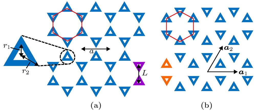
Fig. 1. Schematics of the honeycomb structure of two-dimensional photonic crystals: (a) Triangular lattice structure of “artificial atoms” composed by two equilateral-triangle-ring-shaped silicon rods, which are labeled by purple in the figure, embedded in an air host; (b) the same as pa-nel (a), except that the silicon rods are rotated by 60° around their respective centers, the corresponding “arti-ficial atom” is labeled by orange in the figure.
 and
and
 are unit vectors with length
 a as the lattice constant. The relative permittivity and permeability of silicon rods are
 and
and
 , respectively. The distance from the vertices of the inner and outer equilateral triangles to the center of the silicon rod are
 and
and

 , respectively. The distance between the centers of the neighboring silicon rods is
 . Red hexagons represent the unit cells of the triangular lattices.
and
are unit vectors with length and
, respectively. The distance from the vertices of the inner and outer equilateral triangles to the center of the silicon rod are
and
, respectively. The distance between the centers of the neighboring silicon rods is
. Red hexagons represent the unit cells of the triangular lattices. 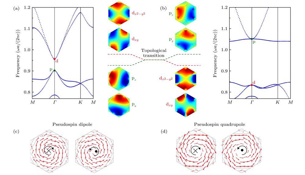
Fig. 2. Band structures and the eigenstates for
 and
and
 irreducible representations: (a) Band structure of P-type photonic cry-stal; (b) band structure of N-type photonic crystal, the insets of (a) and (b) show the magnetic field distributions of the twofold degenerated dipolar state (marked as
 ) and the twofold degenerated quadrupolar state (marked as
 ) at
) at Γ point, and the positive and negative maxima of the magnetic field,
 , are represented by dark red and dark blue, respectively, band inversion takes place under the rotation of the silicon rods; (c) real-space distributions of the time-averaged Poynting vector for the dipolar states in P-type photonic crystal; (d) real-space distributions of the time-averaged Poynting vector for quadrupolar states in P-type photonic crystal; the arrows show the direction and magnitude of the Poynting vector, whose anticlockwise/clockwise circular polarization around the unit cell center reveals the pseudospin-up/pseudospin-down orientation.
and
irreducible representations: (a) Band structure of P-type photonic cry-stal; (b) band structure of N-type photonic crystal, the insets of (a) and (b) show the magnetic field distributions of the twofold degenerated dipolar state (marked as
) and the twofold degenerated quadrupolar state (marked as
) at , are represented by dark red and dark blue, respectively, band inversion takes place under the rotation of the silicon rods; (c) real-space distributions of the time-averaged Poynting vector for the dipolar states in P-type photonic crystal; (d) real-space distributions of the time-averaged Poynting vector for quadrupolar states in P-type photonic crystal; the arrows show the direction and magnitude of the Poynting vector, whose anticlockwise/clockwise circular polarization around the unit cell center reveals the pseudospin-up/pseudospin-down orientation. Fig. 3. Project band structure and topological edge states: (a) Schematic of a ribbon-shaped supercell composed of topologically nontrivial crystal with its two edges cladded by topologically trivial crystals; (b) dispersion relation along ΓK direction for the ribbon-shaped supercell, the ribbon has 20 nontrivial unit cells in the middle and 10 trivial unit cells on both sides, the red and black dots display the edge and bulk states, respectively; (c) distribution of the magnetic field and time-averaged Poynting vector around the lower interface of the supercell, corresponding to point C indicated in panel (b); (d) the same as panel (c), but corresponding to the point D indicated in panel (b); the positive and negative maxima of the magnetic field,
 , are represented by dark red and dark blue, respectively, and the arrows show the direction and magnitude of the Poynting vector.
, are represented by dark red and dark blue, respectively, and the arrows show the direction and magnitude of the Poynting vector. Fig. 4. Two typical interfaces between P-type and N-type photonic crystals: (a) Zigzag interface; (b) armchair interface.
Fig. 5. Unidirectional propagation of the pseudospin-dependent edge states localized at the zigzag interface: (a) Schematic of a point-like chiral source made by an eight-antenna array with phase delay of
 one by one; (b) magnetic field distribution stimulated by the point-like chiral source with an anticlockwise phase delay in the air; (c) magnetic field distribution stimulated by the point-like chiral source with a clockwise phase delay in the air; (d) leftward unidirectional electromagnetic wave propagation excited by the source in panel (b) along the zigzag interface; (e) rightward unidirectional electromagnetic wave propagation excited by the source in panel (c) along the zigzag interface. The structures in panel (d) and (e) are surrounded by the perfectly matched layers; the point-like chiral sources are marked as white circles with operating frequency
 , and their phase delay directions are repre-sented by black arrows; the white arrows along the horizontal direction indicate the propagation directions of the edge states.
one by one; (b) magnetic field distribution stimulated by the point-like chiral source with an anticlockwise phase delay in the air; (c) magnetic field distribution stimulated by the point-like chiral source with a clockwise phase delay in the air; (d) leftward unidirectional electromagnetic wave propagation excited by the source in panel (b) along the zigzag interface; (e) rightward unidirectional electromagnetic wave propagation excited by the source in panel (c) along the zigzag interface. The structures in panel (d) and (e) are surrounded by the perfectly matched layers; the point-like chiral sources are marked as white circles with operating frequency
, and their phase delay directions are repre-sented by black arrows; the white arrows along the horizontal direction indicate the propagation directions of the edge states. Fig. 6. Unidirectional propagation of the pseudospin-dependent edge states localized at the armchair interface: (a) Downward unidirectional electromagnetic wave propagation excited by the point-like chiral source with an anticlockwise phase delay along the armchair interface; (b) upward unidirectional electromagnetic wave propagation excited by the point-like chiral source with a clockwise phase delay along the armchair interface. The structures are surrounded by the perfectly matched layers. The point-like chiral sources are marked as white circles with operating frequency
 , and their phase delay directions are represented by black arrows. The white arrows along the vertical direction indicate the propagation directions of the edge states.
, and their phase delay directions are represented by black arrows. The white arrows along the vertical direction indicate the propagation directions of the edge states. Fig. 7. Robustness of the topological edge states against defects: (a) Magnetic field distribution under the excitation of a plane wave with operating frequency
 in the system consisting of P-type and N-type photonic crystals; (b) the same as panel (a), except that a cavity defect (displayed by ellipse) is introduced into the interface. The structures are surrounded by the perfectly matched layers. Red arrows represent the incident directions. The topological edge states are immune to various defects including sharp bend and cavity at the interface.
in the system consisting of P-type and N-type photonic crystals; (b) the same as panel (a), except that a cavity defect (displayed by ellipse) is introduced into the interface. The structures are surrounded by the perfectly matched layers. Red arrows represent the incident directions. The topological edge states are immune to various defects including sharp bend and cavity at the interface. 
Set citation alerts for the article
Please enter your email address
© Copyright 2018-2021 | Chinese Laser Press. All Rights Reserved 沪ICP备15018463号-20