
Hui Liu, Boyang Xie, Hua Cheng, Jianguo Tian, Shuqi Chen, "Topological photonic states in artificial microstructures [Invited]," Chin. Opt. Lett. 19, 052602 (2021)
- Chinese Optics Letters
- Vol. 19, Issue 5, 052602 (2021)
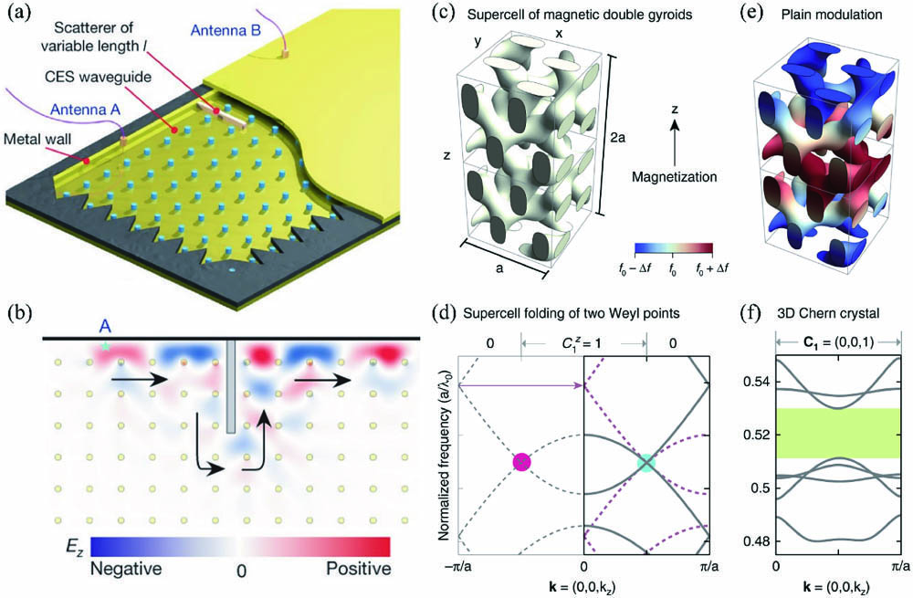
Fig. 1. (a) Experimental setup for a 2D waveguide with gyromagnetic photonic crystal geometry and metal walls. (b) Simulated propagation of chiral edge states around obstacles on the application of a uniform magnetic field. (c) Supercell of the DG photonic crystal magnetized along z. (d) The band structure of 3D Dirac point (blue) folding of two Weyl points (red) in the supercell. (e) The modulation of the supercell period in the z direction. (f) The band structure of the 3D Chern crystal.
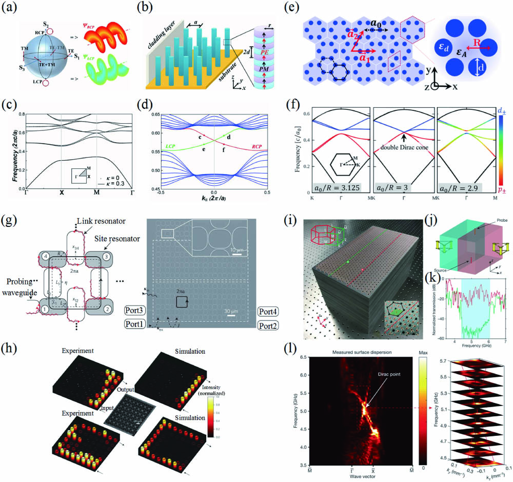
Fig. 2. (a) Polarization on the Poincaré sphere left circular polarization (LCP) (down) and right circular polarization (RCP) (up). (b) Schematic of a quasi-2D superlattice photonic crystal with alternating perfect electric/perfect magnetic layers along the z direction. (c) The band structure of the unit cell without (dotted lines) and with pseudospin coupling effect (solid lines). (d) The projected band structure whose gapless helical edge states for LCP (green line) and RCP states (red line) occur in the topological band gap. (e) Schematic of 2D dielectric photonic crystal of honeycomb lattice. (f) The band structure of the 2D photonic crystals with the lattice constant a0/R
Fig. 3. (a) Schematic of the vortical mirror in Weyl metamaterial. (b) The Weyl metamaterial composed of the metallic saddle-shaped structure. (c) The distribution of ideal Weyl points in Brillouin zone. (d) The overlapped band structures of S1 and S2 planes showing ideal Weyl points. (e) Schematic of the reflection measurement setup in microwave. (f) Reflection phases of the Weyl metamaterial. (g) Schematic of spiraling Fermi arcs. (h) Simulation and experiment of the spiraling Fermi arc at 13.3 GHz. (i) Schematic of 3D photonic Dirac metamaterial. (j) Sample configuration for the experimental measurement. (k) The full wave simulation of 3D photonic Dirac point. (l) Experiment (right) and simulation (left) results of 3D photonic Dirac points along the ky direction. (m) Experiment (right) and simulation (left) results of surface-state arcs at the frequency of Dirac point.
Fig. 4. (a) Schematic of the photonic crystal with kagome lattice. (b) Energy spectrum in trivial and topological regimes. (c) Experimentally measured density of states. (d) Field profile of topological corner states (type I and type II) and edge state. (e) Schematic of the photonic quadrupole topological system. (f) Schematic of the 2D lattice with quadrupole moment. The waveguide couplers are located at the four corners. (g) Energy spectrum with four degenerate corner states in the bandgap. (h) Measured power absorption spectrum at the corners. (i) Spatial intensity profiles showing localized corner modes.


Set citation alerts for the article
Please enter your email address

© Copyright 2018-2021 | Chinese Laser Press. All Rights Reserved 沪ICP备15018463号-20