1Key Laboratory of Radar Imaging and Microwave Photonics, Ministry of Education, Nanjing University of Aeronautics and Astronautics, Nanjing 210016, China
2Shanghai Institute of Satellite Engineering, Shanghai 201109, China
Simin Li, Rong Cong, Zhengqian He, Tianliang Wang, Fangzheng Zhang, Shilong Pan. Switchable microwave photonic filter using a phase modulator and a silicon-on-insulator micro-ring resonator[J]. Chinese Optics Letters, 2020, 18(5): 052501
Copy Citation Text
A switchable microwave photonic filter (MPF) using a phase modulator (PM) and a silicon-on-insulator micro-ring resonator (MRR) is proposed and demonstrated. By adjusting the polarization controller between the PM and the MRR, the filtering function of the MPF can be switched between a band-stop filter and a band-pass filter. In a proof-of-concept experiment, an MPF with a rejection ratio of 30 dB (or 15 dB) for the band-stop (or band-pass) response and a frequency tuning range from 9.6 to 20.5 GHz is achieved.
Microwave photonic filters (MPFs) have shown attractive performance for broadband radio-frequency (RF) applications because of the advantages such as broad bandwidth, flexible tunability, reconfigurability, and anti-electromagnetic interference[1]. In multifunctional RF systems, MPFs with switchable functions between band-pass response and band-stop response are highly desirable. In addition, switchable MPFs are useful when the systems are operated in a complex electromagnetic environment[2,3].
Until now, several switchable MPFs have been proposed, which can be generally classified into three categories. The first approach is realized by changing the tap coefficients of a multi-tap delay line filter. For example, in an infinite impulse response (IIR) MPF based on an amplified recirculating delay line with an in-loop electro-optic modulator (EOM), the band-stop and band-pass responses were implemented by biasing the EOM at the maximum and minimum transmission points, respectively[4]. Another switchable IIR MPF was achieved by a phase modulator (PM), a fiber delay line loop (FDLL), and two tunable optical band-pass filters (TOBFs), which were in and out of the FDLL, respectively[5]. If the two TOBFs were tuned on the same side of the optical carrier, the overall response of the MPF was equal to an all-pass response (determined by a straight-through component) plus a band-pass response (determined by recirculating output taps in the FDLL). Conversely, the two TOBFs were tuned on the opposite sides of the optical carrier, the overall response was equal to an all-pass response minus a band-pass response, and a band-stop MPF was achieved. In these schemes, since there is a huge time delay difference between two adjacent taps, the periodic spectral responses of the multi-tap delay line filter normally have a small free spectral range (FSR), which may limit the filters for wideband applications[6]. The second approach is to manipulate the amplitudes and phases of two optical sidebands by applying an EOM and an optical filter. In Refs. [6] and [7], this was realized by tuning the driving voltages of a dual-drive (DD) Mach–Zehnder modulator (MZM) to employ it in phase modulation or single-sideband (SSB) modulation. Specifically, a phase-shifted fiber Bragg grating was used as the optical filter to suppress one of the sidebands in Ref. [6], while both sidebands were suppressed and amplified, respectively, by the stimulated-Brillouin-scattering (SBS) effect in Ref. [7]. Besides, an MPF with complementary band-pass and band-stop responses was implemented through an integrated polarization-division multiplexing MZM (PDM-MZM) consisting of two dual-parallel MZMs (DP-MZMs) and the SBS effect[8]. By controlling the bias voltages of the two DP-MZMs, the modulated optical signals in the two orthogonal polarizations had asymmetric double sidebands. The SBS effect was performed as an ultra-narrow amplification. The polarizers were employed to adjust the polarization axis of the modulated signal to exhibit an SSB modulation or a phase modulation. In the above scenarios, the DD-MZM or DP-MZM is driven by two quadrature RF signals with the same frequency and amplitude but with a 90° phase offset, and therefore, an electrical 3 dB 90° hybrid exerts an important role in these systems. Because of the small bandwidth of the 3 dB electrical 90° hybrid, the MPFs are also limited for wideband applications. Another method to implement an MPF is mapping an optical filter to a microwave filter[9]. This method employs a switchable optical filter to obtain the switchable function. As the integration of a microwave photonic system is becoming a major trend, the micro-ring resonator (MRR) is regarded as the most promising optical filter solution in the photonic integrated circuits[10]. For a single MRR, despite the drop port and the through port having complementary responses, only one lineshape (band-stop or band-pass) occurs in a certain port. In order to obtain the switchable response in the same output port, some complex MRR-based structures have been put forward, such as reconfigurable cascaded MRRs formed by a programmable two-dimensional (2D) mesh network[11] and a flat-top MRR[12]. In these structures, many parameters should be adjusted precisely through a complex control circuit.
In this Letter, a switchable MPF based on a PM and a normal MRR is proposed and demonstrated, which is easy to operate and features a simple structure. The switchable filtering functions are achieved by adjusting a polarization controller (PC) to manipulate the amplitudes and phases of the optical carrier and two sidebands. This work is an extension of our earlier work reported in Ref. [13]. Here, a comprehensive investigation is conducted, including detailed theoretical analysis and additional experimental results.
Sign up for Chinese Optics Letters TOC. Get the latest issue of Chinese Optics Letters delivered right to you!Sign up now
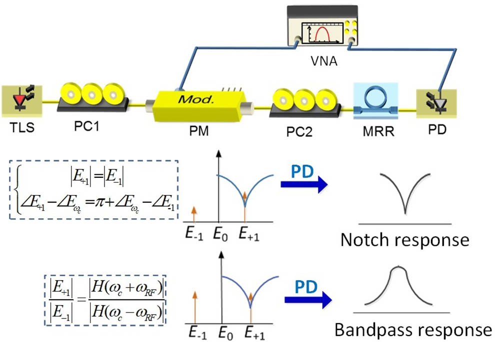
The schematic of the proposed MPF is shown in Fig. 1. An optical carrier from a tunable laser source (TLS) is injected into a PM via the first PC (PC1). The PM has no polarizer at the input port, and PC1 is adjusted to orient the optical carrier’s polarization with a 45° angle with respect to one principal axis of the PM. As a result, the optical carrier is regarded to be equally separated into two orthogonal axes (X and Y polarizations) in the PM. The PM is driven by a microwave signal. Due to the inherent birefringence of the crystal in the PM, a wavelength-dependent phase difference exists between the two orthogonally polarized optical signals[14,15], which can be expressed as where and are the frequencies of the optical carrier and the incoming microwave signal; and are the modulation indexes of the signal along the X axis and Y axis; and are the zero- and first-order Bessel functions of the first kind; is the group index difference of the two orthogonally polarized signals; is the length of the waveguide in the PM; , , and are the wavelengths of the optical carrier and the sideband signal. From Eq. (1), it can be seen that the phase difference between the two polarizations is wavelength dependent.
Figure 1.Schematic diagram of the proposed microwave photonic filter. TLS, tunable laser source; PC, polarization controller; PM, phase modulator without a polarizer; MRR, micro-ring resonator; PD, photodetector; VNA, vector network analyzer.
The output signal from the PM is sent to the second PC (PC2). Then, the optical signal is coupled in a single MRR via a grating coupler on an integrated chip. The grating coupler is designed for TE mode, which means that it can be seen as TE mode polarizers. The MRR on the chip is employed as an optical band-stop filter with a transfer function given by where , are the self-coupling coefficients of the couplers; is the single-pass amplitude transmission coefficient; means the single-pass phase shift; and are the effective refractive index and cavity length of the MRR; and is the light speed. The output signal can be written as where is the polarization angle of the optical chip with respect to the X axis, and is the phase difference between the optical signals along the X axis and Y axis. Both and are determined by the state of PC2. According to Eqs. (1) and (2), the optical carrier and the sideband signals output from the MRR can be expressed as where and denote the amplitude and phase of the corresponding signal determined by the PM and PC2, respectively. Equations (4)–(6) indicate that the amplitudes and the phases of the optical carrier and the RF modulation sidebands can be manipulated by adjusting PC2.
Sign up for Chinese Optics Letters TOC. Get the latest issue of Chinese Optics Letters delivered right to you!Sign up now
Next, the output signal from the chip is sent to a photodetector (PD) to perform optical-to-electrical conversion. The photocurrent after the PD can be described as
To implement a band-stop MPF, the -order optical sidebands at adjusted by PC2 should satisfy
In other words, the -order sidebands have the same amplitude but are out of phase. Consequently, the beat frequency of would be canceled in the PD to present a deep band-stop response at the frequency .
To implement a band-pass MPF, the optical signal adjusted by PC2 should be aligned to the TE mode of the grating coupler, i.e., or . The MRR is applied to suppress one of the phase modulated optical sidebands to perform phase modulation to intensity modulation (PM-IM) conversion. This way, a band-pass response can be obtained.
An experiment is carried out based on the setup in Fig. 1. The MRR employed in the experiment is an add-drop type MRR fabricated on a silicon on insulator (SOI) platform. The length of the MRR cavity is about 1040 μm, corresponding to an FSR of 0.55 nm (i.e., 69 GHz) in the optical transmission spectrum, as reported in Ref. [13]. The magnitude and phase responses of the MRR measured by the SSB modulation optical vector analysis (SSB-OVA) method[16] are shown in Fig. 2, in which the micrograph of the MRR is also displayed. As shown in Fig. 2, the extinction ratio of the MRR is around 13 dB, and the phase shift around the resonant wavelength is nearly 90°. Due to the SSB-OVA having a higher resolution, the extinction ratio measured in this Letter is larger than that measured by the optical spectrum analyzer (OSA, Yokogawa AQ6370C) in Ref. [16]. Based on the measured results and Eq. (2), the self-coupling coefficients ( and ) are estimated to be 0.911, and the single-pass amplitude transmission coefficient is estimated to be 0.95.
Figure 2.Normalized magnitude and phase response of the MRR. Inset: the MRR used in the experiment.
The capability of manipulating the amplitudes and phases of the optical signals by adjusting PC2 is tested. To this end, the grating coupler is used as a polarizer, to which a straight waveguide is connected to avoid the influence from the MRR. An optical carrier is generated by a TLS (Agilent N7714A), and the wavelength is set at 1549.93 nm. The RF signal with a frequency of 14.55 GHz generated by a vector network analyzer (VNA, Keysight, N5235A PNA-L) is applied to the PM (Eospace, PM-DV5-40-PFU-PFU-LV). The output optical signal from the chip is amplified by an erbium-doped optical fiber amplifier (EDFA, Amonics, AEDFA-35-B-FA). Then, a PD (Conquer, KG-PD-50G) is used to complete optical-to-electrical conversion. The optical and electrical spectra are measured by an OSA (APEX, AP2040D) and an electrical spectrum analyzer (ESA, R&S, RS-FSV40-40G), respectively. Figures 3(a)–3(c) show the optical spectra of the SSB modulated signal and the dual-sideband modulated signal obtained via the adjustment of PC2. The intensity of each sideband can be tuned in a range of 20 dB. Figure 3(d) shows the calculated relationship between the power ratio of the and sidebands and the phase factor of PC2 [assume the polarization angle satisfies . It can be seen that the most significant SSB modulations occur when is about and .
Figure 3.(a)–(c) Measured optical spectra of the optical signal output from the chip by adjusting the PC2. (d) The calculated relationship between the power ratio of the and sidebands and the phase factor of PC2.
Then, the capability of manipulating the phases of the sidebands is investigated. By adjusting PC2, the phase difference between the sidebands can be adjusted to be or 0. Correspondingly, the beating results by sending the dual-sideband modulated optical signal to a PD is found to have no RF component and to have an RF component at 14.55 GHz, respectively. As shown in Fig. 4, the maximum power difference of the electrical components is more than 20 dB, while the two optical sidebands keep the same amplitude as shown in the inset figures. It means that the variation of the RF signal is caused by manipulating the phase of the two sidebands.
Figure 4.Measured beat signal spectra of the light output from the chip by adjusting PC2. Inset: the corresponding optical sideband spectra.
To verify the switchable MPF, the MRR takes the place of the straight waveguide. The resonant wavelength locates in the sideband of the modulated signal. The RF signal detected by the PD is fed back to the VNA, which is operating in the sweeping-frequency mode. Figures 5(a) and 5(b) show the simulated (red dash line) and measured (blue solid line) MPF responses via adjusting PC2. Meanwhile, the corresponding optical spectra of the modulated signal at the MPFs’ center frequency are shown in Figs. 5(c) and 5(d), respectively. In both cases, the measured results are almost the same as the simulated results. For the band-stop response, a rejection ratio larger than 33 dB and a 3 dB bandwidth of 8.4 GHz are obtained. The two optical sidebands are equal in magnitude, which agrees with the previous analysis. For the band-pass response, a rejection ratio over 15 dB and a 3 dB bandwidth of 7 GHz are obtained. The optical sideband is lower than the other sideband, which means that the MRR breaks the balance between the two sidebands in phase modulation. As a result, the PM-IM conversion occurs. It should be noted that the response of the band-pass MPF has a poorer rejection ratio than that of the band-stop MPF. This is caused by the fact that the band-stop MPF only requires power cancellation between the frequency components generated by beating the optical carrier with the -order sidebands at a specific input microwave frequency, i.e., the center frequency of the MPF. While, for band-pass MPF, the power cancellation should be achieved in a large microwave frequency range corresponding to the outside of the passband, which is hard to satisfy considering that the amplitude and phase responses at the non-resonant wavelength of the MRR in Fig. 2 are not ideally flat.
Figure 5.Normalized frequency response of the MPF (a) band-stop filter and (b) band-pass filter (solid blue line, measured results; red dash line, simulated results). The optical spectra of the modulated signal at the MPFs’ center frequency: (c) band-stop; (d) band-pass.
The frequency tunability of the MPF is obtained by adjusting the wavelength interval between the optical carrier and the MRR’s resonant wavelength. In this experiment, the wavelength interval is changed by varying the optical carrier. Figure 6(a) illustrates the responses of band-stop MPFs with different center frequencies. It can be seen that when the center frequency is tuned from 9.6 GHz to 20.5 GHz, the MPFs have similar profiles and a nearly fixed 3 dB bandwidth of ∼8 GHz. The rejection ratios are over 30 dB with a maximum value of 39 dB. When the center frequency becomes increasingly higher, such as 27.6 GHz, the rejection ratio is decreased to 23 dB, and the 3 dB bandwidth is broadened to over 10 GHz. In this case, the optical carrier is away from the operative resonant wavelength of the MRR but close to its adjacent resonant wavelength. Thus, the -order sideband is affected by the response of the adjacent resonant wavelength. As a result, insufficient cancellation between the -order phase modulation sidebands occurs, leading to a reduced rejection ratio and a broadened 3 dB bandwidth. Figure 6(b) shows the responses of band-pass MPFs in the same frequency range. The rejection ratios when the center frequency changes from 9.6 GHz to 20.5 GHz are larger than 15 dB with a similar profile. While, for a similar reason with that in Fig. 6(a), the response for further higher center frequency (27.6 GHz) suffers from a reduced rejection ratio, which limits the tuning range of the MPF.
Figure 6.Normalized frequency responses of the MPFs with different center frequencies when the MPF is operating as (a) the band-stop filter and (b) the band-pass filter.
It should be noted that the frequency responses of the MPFs are determined by the PC together with the MRR. Applying a high-accuracy PC and MRR with high Q value and large FSR will help to improve the performance of the proposed switchable MPF like rejection ratio, bandwidth, and frequency tuning range.
In conclusion, a simple switchable MPF using a PM and an SOI MRR is proposed and experimentally demonstrated. The switchable function of the system is realized by adjusting the PC between the PM and the MRR to manipulate the amplitudes and phases of the optical signals. A switchable MPF with a rejection ratio of 30 dB (or 15 dB) for the band-stop (or band-pass) response is demonstrated. In virtue of tuning the wavelength of the optical carrier, the center frequency of the MPF can be tuned from 9.6 GHz to 20.5 GHz.
Simin Li, Rong Cong, Zhengqian He, Tianliang Wang, Fangzheng Zhang, Shilong Pan. Switchable microwave photonic filter using a phase modulator and a silicon-on-insulator micro-ring resonator[J]. Chinese Optics Letters, 2020, 18(5): 052501