
Beibei Guo, Yaoming Wang, Xiaolong Zhu, Mingsheng Qin, Dongyun Wan, Fuqiang Huang, "Molybdenum thin films fabricated by rf and dc sputtering for Cu(In,Ga)Se2 solar cell applications," Chin. Opt. Lett. 14, 043101 (2016)
- Chinese Optics Letters
- Vol. 14, Issue 4, 043101 (2016)
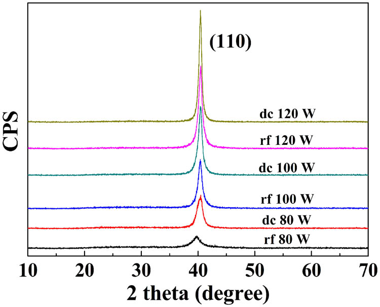
Fig. 1. XRD patterns of as-deposited Mo films prepared by dc and rf magnetron sputtering, respectively, as a function of the supplied power.
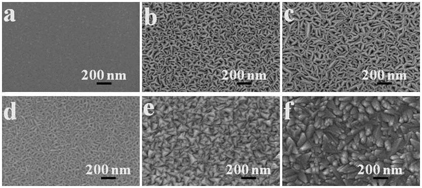
Fig. 2. SEM images of the Mo films prepared by dc and rf magnetron sputtering, respectively, with different supplied powers: (a) rf 80 W, (b) rf 100 W, (c) rf 120 W, (d) dc 80 W, (e) dc 100 W, and (f) dc 120 W.
Fig. 3. AFM images of the Mo films prepared by dc and rf magnetron sputtering, respectively, with different supplied powers, revealing the differences in grain size and morphology: (a) rf 80 W, (b) rf 100 W, (c) rf 120 W, (d) dc 80 W, (e) dc 100 W, and (f) dc 120 W.
Fig. 4. Cross-sectional SEM images of the Mo films deposited at 100 and 120 W by rf and dc sputtering, respectively: (a) rf 100 W, (b) dc 100 W, (c) rf 120 W, (d) dc 120 W. (e) Bright-field TEM micrograph from the dc-120 W Mo film.
Fig. 5. (a) SEM cross-sectional image of the glass/Mo/CIGS sample after selenization, (b) I-V characteristic of the CIGS solar cells.
|
Table 1. Structural and Electrical Properties of the As-Deposited Mo Films


Set citation alerts for the article
Please enter your email address

© Copyright 2018-2021 | Chinese Laser Press. All Rights Reserved 沪ICP备15018463号-20