• Chinese Journal of Lasers
  • Vol. 50, Issue 1, 0113009 (2023)
Yuexing Xia1、2, Shuai Zhang1、2, Keming Wu1, Yiyang Gong1、2, Shuai Yue1、2、*, and Xinfeng Liu1、2、**
Author Affiliations
  • 1CAS Key Laboratory of Standardization and Measurement for Nanotechnology, National Center for Nanoscience and Technology, Beijing 100190, China
  • 2University of Chinese Academy of Sciences, Beijing 100049, China
  • show less
    DOI: 10.3788/CJL221252 Cite this Article Set citation alerts
    Yuexing Xia, Shuai Zhang, Keming Wu, Yiyang Gong, Shuai Yue, Xinfeng Liu. [J]. Chinese Journal of Lasers, 2023, 50(1): 0113009 Copy Citation Text show less

    Abstract

    In recent years, two-dimensional (2D) materials have attracted extensive interests due to the large exciton binding energy different from bulk materials. Many peculiar properties have been discovered that have far-reaching perspectives in the next generation of optoelectronic devices. In this review, we introduce the forms of exciton existence in 2D materials and several promising 2D materials with good applications at first. Then, we summarize relevant contemporary tools for probing exciton dynamics and methods of regulating 2D exciton transport, for instance, electrical regulation, stress/surface wave regulation and moiré potential regulation, etc. Finally, we conclude the general development of regulation in 2D materials and propose several possible opportunities of application prospect.In recent years, two-dimensional (2D) materials have attracted extensive interests due to the large exciton binding energy different from bulk materials. Many peculiar properties have been discovered that have far-reaching perspectives in the next generation of optoelectronic devices. In this review, we introduce the forms of exciton existence in 2D materials and several promising 2D materials with good applications at first. Then, we summarize relevant contemporary tools for probing exciton dynamics and methods of regulating 2D exciton transport, for instance, electrical regulation, stress/surface wave regulation and moiré potential regulation, etc. Finally, we conclude the general development of regulation in 2D materials and propose several possible opportunities of application prospect.

    1 Introduction

    The charge and energy transfer properties are essential in semiconductors1. In general,we characterize these properties by carriers or excitons. Carriers mainly include free electrons and holes. Exciton is a quasi particle which is formed by a pair of electrons and holes that are attracted to each other. In 2D semiconductor materials,excitons are of wide interest due to their particularly large binding energy. Under the excitation of light,valence band electrons are excited to the conduction band and subsequently bound together by the Coulomb force between electrons and holes to form electron-hole pairs. The bound electron-hole pairs are very similar to hydrogen atoms,and therefore their exciton energy level distribution is also similar to that of hydrogen atoms,which can be described by the hydrogen-like Rydberg model.

    Since the first mechanical exfoliation of graphene from graphite by Geim in 20042,2D materials have received a lot of attention. Subsequently,due to their unique properties and promising applications,a large number of new 2D materials have surpassed graphene in terms of application potential,such as transition metal dihalides(TMDCs,including MoS2,MoSe2,MoTe2,WS2,WSe2,ReS2,TaS2,etc.)3-5,and hexanol boron nitride(h-BN)6-7. Due to their ultrathin properties,the novel physical,optical,and electronic properties possessed by 2D materials are expected to have far-reaching effects in the fields of nano-electronics,nano-photonics,nano-sensing and nano-devices8-12.

    The exciton binding energy of 2D semiconductor materials is usually particularly large due to the weakening of Coulomb shielding effect13,for example that of a single layer of WS2 is about 0.7 eV14,and that of a single layer of black phosphorus is up to 0.9 eV15. Theoretical analysis shows that the exciton binding energy for 2D materials is at least ten times higher than that for bulk materials16. The large exciton binding energy means that the spectral properties of the material are generally determined by the exciton properties. Meanwhile,many higher-order exciton effects,such as trion and biexciton formation,are likely to be particularly important17.

    Therefore,the study of exciton dynamics in 2D materials is of great significance. However,a systematic overview of the relevant regulating methods has rarely been reported. In this review,we focus on several emerging classes of 2D materials and their heterostructures. Firstly,we introduce the intrinsic principles of exciton diffusion in 2D materials and the tools to probe exciton diffusion. Then,we review the electrical regulation,stress/surface wave regulation,moiré potential regulation and some other potential regulating methods of exciton diffusion in recent years. Finally,we summarize the recent research,and provide some discussion of the challenges and prospects in the future.

    2 Intrinsic Principle of Exciton Diffusion

    There are two typical cases of exciton states in semiconductors:one is the Frenkel exciton,where the electron-hole pair binding energy is large and the exciton Bohr radius is small and localized to the molecule18-19;the other is the Wannier-Mott exciton,where the electron-hole pair binding energy is small and the Bohr radius is much larger than the lattice constant20-21. In molecular crystals,most excitons belong to Frenkel exciton and are transported by hopping between localization sites,while in semiconductors,most excitons belong to Wannier-Mott exciton and exhibit semi-classical free-particle transport22. In 2D semiconductor materials,excitons are delocalized but have strong binding energy,which means both properties of transport will be present in it,especially in TMDCs23.

    In semiconductors,we usually use Einstein relation to describe exciton diffusion24-25. Using the random walk model,we can derive that the ratio of diffusion coefficient D to the mobility μ is constant and satisfies the Einstein relation:

    D=μkBTq

    where kB represents the Boltzmann constant,T is the Kelvin temperature,and q is the elemental charge26. However,Einstein relation has its limitation. When the temperature reaches a certain level and the band transport in the semiconductor is beyond the Boltzmann distribution,this relation needs to be complemented more systematically27. More in-depth simulations and discussions were reported by Baranovskii et al.28. And in most cases,we generally keep the temperature within the range that satisfies Einstein relation.

    To further understand the exciton diffusion in 2D materials with carrier lattice interactions,a large number of theoretical and experimental researches have been carried out29-30. At an earlier interaction timescale,that is,before exciton formation,carrier-carrier scattering is one of the key factors affecting carrier transport31. When a large number of photogenerated carriers are excited at high energy,they will undergo a carrier-carrier scattering process to form quasi-free hot carriers. This thermalization process is completed in only 20 fs and will be followed by a cooling process around 500 fs,namely the transfer of energy to the lattice through electro-phonon coupling,which accompanies the formation of excitons32. Liu et al.33 directly captured the spatiotemporal dynamics of the transition from hot carriers to bound-excitons. In this progress,a rapid thermal expansion in diffusion is present,followed by a transition into negative diffusion and finally into linear exciton diffusion. After exciton formation,the movement of exciton is scattered by the optical phonon,impurity induced ionization and other excitons. The decisive factor in the intrinsic mechanism of charge transport originates from the interaction of carriers with lattice vibrations34. By calculating the carrier-phonon scattering rates following Fermi’s golden rule in different monolayer MX2 (M=W,Mo;X=S,Se)of similar structure,effects other than lattice vibrations are excluded. The results show that the scattering rates of electrons change abruptly as the phonon interaction increasing,which means that the phonon interaction determines the electron transition. In addition,another study showed that at low excitation densities,exciton diffusion shows a Gaussian distribution,satisfying the conventional Fick’s law,but at strong excitation densities,thermo-optical phonons can seriously affect the pair exciton scattering,making the exciton diffusion show a super-Gaussian distribution35. These are strong evidence that phonon scattering plays a decisive role. However,real materials contain not only exciton phonon scattering processes,but also defects which are often present in the materials. Due to the injection of defects,electron interactions create dielectric disorder,which largely affects exciton transport in 2D materials36. By using ultrafast microscopy,the presence of defects can cause neutral excitons to be trapped in 2D materials. Subsequently,the defect-bound exciton will relax through the nonradiative exciton,and the lifetime and diffusion coefficient of the exciton decrease abruptly37-38.

    Due to the short lifetime of excitons and the aforementioned effects of phonon scattering and defect compounding,it is not easy to test the exciton transport experimentally. In this article,the favorable tools for probing the exciton transport properties mainly include time-resolved photoluminescence(TRPL)spectroscopy39-41 and ultrafast transient absorption microscopy(TAM)42-44. For TRPL,the sample fluorescence is excited by a femtosecond laser,and the population distribution of the fluorescence at different time is obtained by an avalanche photodiode(APD)or streak camera. Then the diffusivity is obtained by the relationship between population distribution and diffusion time. Different from TRPL,TAM obtains time-resolved absorption signal by pump-probe technique. Depending on the thickness of the sample,TAM can freely select the reflected or transmitted absorption signal. Similarly,the diffusivity of the carriers in it can be analyzed by the distribution of the population. Both tools for detecting exciton diffusion are achieved by collecting spectra. TRPL does not require strict flatness of the sample and can achieve picosecond diffusion detection by detecting the fluorescence emitted by exciton recombination. TAM requires higher flatness of the sample,whether it is reflective or transmissive probe,and ultimately the signal of exciton or carrier transport is calculated by the difference spectrum before and after the pump. This method can obtain shorter scale diffusion processes and can be applied for the processes prior to exciton-phonon scattering.

    Population distribution corresponds to the diffusion length. The specific principle is traced back to the intrinsic diffusion equation,with the probability density distribution satisfying

    nx,tt=D2nx,tt2-nx,tτ

    where τ is the decay time constant which can be solved by Fourier transforming into the momentum space. For a given initial density distribution nx,0,the population distribution nx,t is a convolution of the initial distribution nx,0 with the time-dependent Gaussian function,

    nx,t=exp-t/τ14πDt-+nx,0exp-x-x024Dtdx

    where x0 is the center of the initial distribution.

    In most cases,the initial distribution can be fitted by a Gaussian distribution. Through the initial distribution,the peak density n0 and the initial spatial variance σ02 can be identified. So,the final expanding Gaussian distribution is

    nx,t=exp-t/τn0σ02σ02+2Dtexp-(x-x0)24Dt+2σ02

    in which the spatial variance σ2=σ02+2Dt.

    Finally,the mean square displacement(MSD)DMS grows linearly with time:

    DMS=xt2-x02=σ2-σ02=2Dt.

    The MSD equation indicates the relationship between population distribution and diffusivity. Most researchers study carrier diffusion phenomena by characterizing the diffusivity in this way45. The population distribution of the fluorescence or absorption signal is measured by TRPL or TAM,and then the MSD is obtained by fitting the Gaussian distribution.

    It can be concluded that by the above tools,we can obtain the diffusivity of carriers in any materials. However,the carrier transport process is not always smooth. In general,the carrier transport process is affected by electron-phonon coupling and defect scattering46-48. Typically,when the carriers come to the edge,the situation can be very different from the inside case. With the assist of the edge state,the electron can break free from the exciton binding energy and dissociate into a free carrier49. These show that exciton transport in 2D materials is a worthy challenge. Understanding and regulating exciton diffusion in 2D materials is of great importance.

    3 Methods of Regulating Exciton Diffusion

    Regulation of exciton diffusion has attracted much attention in recent years. The ability to freely control the exciton transport behavior is useful for understanding exciton dynamics processes in 2D materials and for applications in optoelectronic devices. We mainly consider the transport dynamics regulated by exciton itself and surrounding environment. Regulation by exciton itself mainly uses bias electric field to change the kinetic energy(acceleration)or self-energy(trion)of the exciton. Regulation by surrounding environment mainly uses strain to influence the potential field around the exciton or to build a new potential field(moiré potential). So,we have chosen to discuss these types of regulation. In terms of applications,the most common method of regulation is to apply electric field. For optoelectronic devices,external stress is also a major factor affecting the performance and lifetime of the device. Understanding the effect of applied stress on exciton diffusion can provide assistance to improve device stability. At the same time,applying it to modulate diffusion can further optimize the design of future devices. In addition,the moiré potential is the properties of the material itself,and the regulation method using its own properties is beneficial for applying the material to any scenario. Finally,we summarize some other modulation means,all of which have some influence on the diffusion and are worth taking into account when regulating the exciton diffusion.

    3.1 Electrical Regulation

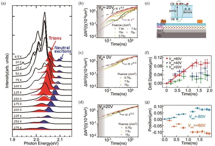
    Because of the simple response of carriers to electric fields,regulation of carrier transport by electric fields is the most common method. In 2008,High et al.50implemented control of exciton flux in an excitonic integrated circuit. They formed interlayer excitons by coupling quantum wells,the lifetime of which is usually 10 ns to 10 ms51-53,solving the usual problem of short lifetime during exciton transport. However,their experimental environment is still at low temperature,which means that realizing regulation of exciton transport at room temperature is difficult. 2D materials solve such a problem due to the large exciton binding energy,so that they have a wide range of prospects. Spatial confinement and Coulomb shielding cause the large exciton binding energy in 2D materials,which makes exciton transport at room temperature easier. In addition,interlayer excitons,unique in 2D materials,have longer lifetimes than intralayer excitons. The long lifetime is of great use for optoelectronic devices. What’s more,2D materials are highly advantageous in ultrathin semiconductor devices,so it is of great interest to study the carrier dynamics modulated by electric field. Experiments have shown that in the presence of an electric field,excitons tend to combine with a positive hole or a negative electron to form trion54-55. Trions are more pronounced in monolayer 2D materials compare with conventional semiconductors56. Thus,the control of the electric field on the trion transport in monolayer 2D materials has far-reaching implications for the next generation of optoelectronic devices.

    To understand the transport dynamics of neutral exciton and trion,Kato et al.57 reported exciton diffusion dynamics over a wide temperature range. Figure 1(a)shows the photoluminescence(PL)spectra of monolayer WS2 at different temperatures. The main components can be separated by fitting the PL peak width. At low temperatures(<75 K),the trion peak dominates. As the temperature increases(75-200 K),the trion peak decays and the neutral exciton peak gradually increases. At high temperatures(>200 K),there is almost no trion peak and the neutral exciton peak dominates. At low temperatures,due to the weakening of phonon scattering,neutral excitons collide with electrons or holes during diffusion to form trions. At that time,the diffusion of neutral excitons varies linearly with increasing temperature. At moderate temperatures,with the increase of thermally activated neutral exciton concentration,ionized impurity scattering becomes the main factor to inhibit the diffusion of neutral excitons. At high temperatures,longitudinal optical(LO)phonon scattering suppresses trion formation,so that the PL spectrum is dominated by neutral excitons. At the same time,the diffusion of neutral excitons is also suppressed due to phonon scattering. Their research showed the temperature dependence of trion and neutral exciton transitions. The transition process of trions and neutral excitons in electrically controlled carrier transport is very peculiar,and Ross et al.58 reported that process. Due to the injection of electrons or holes,the probability of the neutral excitons binding into trions is increasing. Recently,the trion to exciton transition has been achieved by orbital angular momentum light at low temperatures59,which also serves as an inspiration for future studies on trions and is expected to provide a platform for many-body interactions.

    Transition and electrical control of neutral exciton and trions in 2D materials. (a) PL spectrum of monolayer WS2 at 4.5-275 K, where the blue and red parts are fitted to the neutral exciton and trion components, respectively[57]; (b)-(d) MoS2 PL intensity distribution variance as function of time at different back-gate voltage (Vg=-20, 0, 20 V)[60]; (e) trion formation and schematic diagram of the monolayer WS2[61]; (f) drift distances of the trions as function of the dacay time at different applied bias (Vext=20, 40, 60 V)[61]; (g) the peak position of the PL emission as function of decay time at applied bias Vext=-60 V and 60 V[61]

    Figure 1.Transition and electrical control of neutral exciton and trions in 2D materials. (a) PL spectrum of monolayer WS2 at 4.5-275 K, where the blue and red parts are fitted to the neutral exciton and trion components, respectively[57]; (b)-(d) MoS2 PL intensity distribution variance as function of time at different back-gate voltage (Vg=-20, 0, 20 V)[60]; (e) trion formation and schematic diagram of the monolayer WS2[61]; (f) drift distances of the trions as function of the dacay time at different applied bias (Vext=20, 40, 60 V)[61]; (g) the peak position of the PL emission as function of decay time at applied bias Vext=-60 V and 60 V[61]

    Based on the understanding of the transition between trions and neutral excitons,Uddin et al.60 and Cheng et al.61 reported,respectively,the diffusion of neutral excitons and negative trions in monolayer TMDC. Figures 1(b)-1(d)show the diffusion of neutral excitons in monolayer MoS2 at different back-gate voltage. The diffusion coefficient can be given by the intensity distribution variance as

    Δω2t=Atα

    where A is the empirically observed proportionality factor and the exponent α is the diffusion character. α<1 means the transport is subdiffusive and α=1 means the normal diffusion. It is not difficult to find that at 0 and 20 V,the neutral exciton exhibits subdiffusive behavior and the diffusion distance does not vary significantly with pump power. While Vg=-20 V,the transport process of neutral excitons changes from normal diffusion to subdiffusion with increasing pump power. The subdiffusion process is understandable,which stems from the fact that the presence of trions disrupts the transport of neutral excitons. However,at -20 V,excitons mainly undergo the process of radiative recombination at low pump power,leading to normal diffusion,while biexciton dominating recombination dynamics at high pump power requires further confirmation. Figure 1(e)shows the trion formation and structure schematic of monolayer WS2. The electrical tuning of trion diffusion is shown by Figs. 1(f)and 1(g). As the bias voltage increases,the diffusion distance increases first and saturates later,and the diffusion distance keeps increasing. In contrast,the diffusion of trions at two completely opposite bias voltages is not the same,which is similar to the behavior of neutral exciton diffusion described above. Meanwhile,the positive and negative electrical tuning of interlayer excitons in bilayer MoS2 reported by Peimyoo et al.62 also has some deviations. Therefore,it is reasonable to assume that there are other special many-body interactions in this process. In addition,by comparing the monolayer and bilayer TMDCs,we can easily find that the transition from exciton to trion becomes complicated. If we can detect the interlayer exciton and intralayer exciton separately in the subsequent research,it may be helpful for 2D optoelectronics and quantum informatics.

    The properties of a single material are always limited. Currently,the more popular material is van der Waals heterostructure,about which we will describe in detail later. There are also many applications of electric field modulation on such structures,but most of them are for the study of interlayer exciton transport,with few reports on trion correlation63. The separation of neutral excitons and trions by electrical regulation is expected to have broad implications for future exciton devices.

    3.2 Stress/Surface Wave Regulation

    During the preparation and application of electronic devices,strain forces are inevitably generated on the material. How to recognize the effect of stress on exciton transport in 2D materials and to apply it skillfully becomes a topic worthy of consideration. Currently,the effect of strain on 2D materials is mainly studied by applying pressure to both sides of the 2D material to produce tensile strain64-67,or by applying pressure through the tip of a needle to produce exciton funneling68-70. It is also possible to generate biaxial strain by stretching the sample through the thermal expansion of the substrate,although temperature can have an effect on the thermal expansion of the 2D material itself71. The above processes are limited in their control of strain,and it would be difficult to achieve overall strain regulation throughout a 2D material. Recently,the control of exciton flow transport by surface acoustic waves(SAWs)has been reported72-73,which is likely to influence and provide guidance for future modulation of exciton transport by strain.

    TMDC,by virtue of its high sensitivity to external strain,is well suited for room temperature directed transit of direct excitons under dynamic strain only. Datta et al.72reported the regulation of excitons in monolayer WSe2 by SAWs at one direction recently. As the SAWs oscillate forward,the spread of excitons also shows a tendency to oscillate forward. The source of the oscillation is the oscillating potential of the exciton corresponding to the dynamic strain field at different time. We can interpret this process as a continuous wave-powered exciton spreading forward. Although modulation by SAWs in one direction is hard enough,to cover the whole 2D material,modulation of excitons in two directions is still expected. At present,a full range of SAWs modulation excitons at low temperatures has been achieved73. Figure 2(c)shows the schematic illustration of the h-BN encapsulated bilayer WSe2 stacked on SAW devices. When the SAWs are turned off,the exciton exhibits normal diffusion and its diffusion is proportional to DNexx. The distance of exciton and the laser is only 1-2 μm[Fig. 2(a)]. When the SAWs are turned on with Ps=6 mW,the exciton moves away from the position of the laser,and the diffusion distance is about 20 μm,as shown in Fig. 2(b). Comparing the diffusion between the on and off states,directional transport of excitons at any point in a 2D material can be expected. This provides a wealth of functionality and flexibility for future phonon electronic devices. Besides,both of the above-mentioned articles place samples on substrates like LiNbO3. LiNbO3,as an excellent electron-phonon coupling material,has great potential for future modulation of exciton transport.

    Control of exciton flux by SAWs at room temperature. (a),(b) Real-space PL mapping of bilayer WSe2 when SAW is off (a) and when SAW is on with 6 mW power (b); (c) schematic illustration of hBN encapsulated bilayer WSe2 stacked on SAW devices[73]. (d) Schematic of strain induced diffusion of excitons in monolayer WS2; (e) large diffusion length due to exciton-exciton annihilation by one exciton providing additional kinetic energy to another; (f) diffusion length of neutral excitons as function of generation rates in monolayer WS2 at different strains (ε=0, 0.5%)[75]

    Figure 2.Control of exciton flux by SAWs at room temperature. (a),(b) Real-space PL mapping of bilayer WSe2 when SAW is off (a) and when SAW is on with 6 mW power (b); (c) schematic illustration of hBN encapsulated bilayer WSe2 stacked on SAW devices[73]. (d) Schematic of strain induced diffusion of excitons in monolayer WS2; (e) large diffusion length due to exciton-exciton annihilation by one exciton providing additional kinetic energy to another; (f) diffusion length of neutral excitons as function of generation rates in monolayer WS2 at different strains (ε=0, 0.5%)[75]

    In addition to the modulation of exciton transport by SAWs,the use of stress-generated strain can also manipulate exciton transport behavior. Due to the lattice-distortions and the multi-valley excitonic landscape,the variation of diffusion with strain is not linear,where multibody interactions should be considered74. Uddin et al.75 reported the effect of exciton-exciton annihilation(EEA)on diffusion in monolayer WS2 recently. Figure 2(d)shows the schematic of the strain device. Strain was applied by a two-point bending method. Due to its flexibility and thermal stability,polyimide substrate was chosen as the strain platform. However,in as-exfoliated monolayer,due to native sulfur vacancies,neutral excitons are likely to recombine into negative trions. So,the diffusion length of as-exfoliated monolayer WS2 in Fig. 2(f)exhibits a short distance near 200 nm. To ignore the influence caused by trions,they employed chemical counterdoping to detect neutral excitons only. Figure 2(e)shows their understanding of exciton-exciton annihilation. A hot exciton crashes into a cold exciton and loses its kinetic energy. Then the hot exciton transfers into a cold exciton and emits luminance. From Fig. 2(f),it is seen that the strained monolayer will lead to EEA suppression,so the diffusion length shows no dependence on the generation rates. So,strain modulation can enhance the neutral exciton diffusion by suppressing EEA,which also affects the PL quantum yield. Based on the above research,in the case of applied strain,it is likely that there are other ultrafast processes or interactions arising that are worthy of follow-up research.

    3.3 Moiré Potential Regulation

    The van der Waals heterojunction stacked by TMDCs is the current mainstream heterostructure76. Since it was proven that two different 2D materials can be freely stacked,a lot of research has been devoted to this new field. The basic principle is simple:add one single-layer 2D crystal on the top of another single-layer 2D crystal. Strong covalent bonds provide in-plane stability of 2D crystals,whereas relatively weak,van-der-Waals-like forces are sufficient to keep the stack together. However,due to the mismatch in the lattice constants of the two materials composing the heterostructure,moiré pattern with longer periodicity than each layer is generated in the plane and form a moiré superlattice,while a nanoscale periodic potential field is introduced between the layers77-78. In most cases,TMDCs heterostructures have a type II band arrangement with the extreme points of the conduction and valence bands located in different material layers79-80. For example,in the MoS2/WS2 system,the conduction band minimum(CBM)is located at MoS2 and the valence band maximum(VBM)is located at WSe2. The electrons in CBM and holes in VBM of the different layers comprise interlayer excitons,which possess a longer lifetime than the intralayer excitons81,leading to ultrafast excitons transfer82-84. The dynamics and diffusion properties of the moiré exciton can be controlled by varying the twist angle85-87. In addition,controlling the repulsive dipole interaction by changing the interlayer distance can influence the moiré potential energy and thus regulate the bright exciton transport88.

    In TMDCs heterostructures,the applied periodic potential field introduced by the material lattice mismatch or the relative interlayer twisting is called exciton moiré potential. It can regulate the physical properties of the interlayer excitons in the TMDCs system89. With different twist angles near 0° and 60°,shown in Figs. 3(a)and 3(b),the moiré potentials of interlayer exciton are divided into H-type and R-type90. Interlayer excitons are trapped in the local minima without any interactions. As a result,by changing the twist angle of the heterostructures,as shown in Fig. 3(c),the diffusivity of interlayer exciton will be changed. Besides,as the temperature increases,the average diffusivity of interlayer excitons increases linearly,which means that interlayer excitons absorb thermal energy and thus cross the moiré potential barrier. Based on the above-mentioned experiments,results similar to the research of Yuan et al.87 can be obtained:

    D=D0exp(-UmoirékBT)

    Interlayer exciton transport modulated by moiré potentials. (a),(b) Schematic plot of the moiré potential in MoSe2/WSe2 heterostructures, with twist angles near 0° (H-type) and 60° (R-type); (c) interlayer exciton diffusivity as function of temperature with twist angles of 0.15° (purple), 2.49° (green), 5.12° (yellow), and 53.9° (blue)[89]. (d) Illustration of different stackings from hBN/graphene moiré superlattice; (e) MSD of exciton density distribution in bare WSe2 on SiO2/Si substrate (blue dots), PDMS-WSe2 on SiO2/Si substrate (black diamonds) and hBN encapsulated WSe2 (red squares), where inset plots diffusivities as function of time for three samples; (f) comparison of exciton diffusivities with and without graphene layer[91]

    Figure 3.Interlayer exciton transport modulated by moiré potentials. (a),(b) Schematic plot of the moiré potential in MoSe2/WSe2 heterostructures, with twist angles near 0° (H-type) and 60° (R-type); (c) interlayer exciton diffusivity as function of temperature with twist angles of 0.15° (purple), 2.49° (green), 5.12° (yellow), and 53.9° (blue)[89]. (d) Illustration of different stackings from hBN/graphene moiré superlattice; (e) MSD of exciton density distribution in bare WSe2 on SiO2/Si substrate (blue dots), PDMS-WSe2 on SiO2/Si substrate (black diamonds) and hBN encapsulated WSe2 (red squares), where inset plots diffusivities as function of time for three samples; (f) comparison of exciton diffusivities with and without graphene layer[91]

    where kB is known as the Boltzmann constant,T is the temperature,D0 denotes the bare diffusivity,and Umoiré is the moiré potential energy. On the basis of the report of Ref.[89],it can be confirmed that adjusting the moiré potential by twisting the angle is an effective method of regulating exciton diffusion. However,exciton diffusion in heterogeneous junctions is not so simple. Due to the interplay between the moiré potentials and strong many-body interactions,the diffusion of interlayer excitons is anomalous. There are still many unknown interactions in this process that need to be interpreted.

    In addition to changing the twist angle,adjusting the distance between layers and the dielectric surroundings can also cause a variance in moiré potential91. Figure 3(d)shows the calculated dielectric constants of three different stacking samples of hBN/graphene moiré superlattice. Through dielectric perturbation,moiré stripes will be generated in WSe2. The MSDs of the exciton density distribution in bare WSe2 on different dielectric surroundings are shown in Fig. 3(e). It is not difficult to find that in the hBN-encapsulated WSe2,the exciton shows normal diffusion. However,for the other two,the exciton shows subdiffusion. Li et al.91 attributed this to different dielectric perturbations leading to different moiré potential trap depths. Besides,the effect of the dielectric surroundings on the moiré potential can also be obtained by comparing the diffusivity with and without graphene[Fig. 3(f)]. When graphene is present on the top,the moiré superlattice experiences larger dielectric disorder,causing the larger moiré potential. Thus,the diffusivity increases from 0.72 to 0.85 when there is no graphene on the top. Although their work mainly explored WSe2 entrapped among other materials,they provided a probable method to modulate the moiré potential. Based on this method of regulation,we can consider the possibility of dielectric environment in 2D heterostructures for regulation.

    Because the modulation of angle or surrounding is not easy,the effect of altering the moiré potential by twist angle or interlayer distance on exciton transport is limited. On the basis of modulating the moiré potential,manipulating the localization-delocalization transition of the interlayer excitons by using an applied electric field,active modulation of their spatial diffusion behavior is expected92. In addition,the existence of moiré intralayer excitons at low temperatures was recently confirmed in the WSe2/WSe2 homobilayer system93,which is expected to modulate the intralayer excitons through the moiré potential,providing new opportunities for quantum emitters and photoelectronic devices. Actually,intralayer charge-transfer excitons in moiré superlattices have just been reported94. In addition to the common interlayer Wannier-type exciton,Naik et al.94 found an intralayer charge-transfer exciton in which the electrons and holes are separated by about 5 nm. Based on their study,we can focus on the diffusion of intralayer excitons. Besides,the interactions between intralayer and interlayer excitons can also be discussed,and perhaps these two types of excitons directly also undergo fantastic processes that have implications for future novel modulated nanodevices and solar cells.

    3.4 Other Regulations

    Apart from the above-mentioned widely studied modulators,there are actually some other methods of regulating exciton dynamics.

    Varying the excitation power and the temperature is a universal method. It has been reported that,at low excitation power,excitons show subdiffusion because of the presence of defect states,while at high excitation power,the exciton density increases and the defective states are filled,so that they show normal diffusion,which is totally different from TMDCs95. Besides,in their research,the intrinsic diffusivity show a sensitive dependence on the stiffness of the lattice by measuring of different types of 2D perovskites95.

    Changing the number of layers is also a recently common method,especially in heterostructures. Conventional TMDCs out-of-plane heterojunctions use two different layers of materials. Producing more intralayer excitons by increasing the thickness of one layer can enhance the correlation between the intralayer and interlayer excitons,which will lead to more interesting transport processes96. Adding a layer of another material between two identical materials is a method to change the layer numbers,such as MoSe2/MoS2/MoSe2 trilayer heterostructure97. In this case,the number of interlayer excitons increases and they prefer to combine to form interlayer trions. On this basis,the research may provide insights into future photoelectronic applications by means of electrical modulation,etc.

    2D material is a good platform for valley exciton dynamics. Because the monolayer structure of 2D materials breaks the spatial inversion symmetry and the material has strong spin-orbit coupling,a unique spin-valley locking effect is formed. However,the spin-valley exciton dynamics in 2D materials is very complex. Different physical mechanisms such as many-body effects of electron-hole interactions,electro-phonon coupling and spin-orbit coupling are involved98-99. So,the regulation of valley exciton diffusion still requires considerable theoretical and experimental investigation. Currently,the diffusion dynamics of valley exciton diffusion in a large-scale monolayer WSe2 is reported. Wang et al.100 achieved the characterization of valley exciton diffusion by transient grating spectroscopy,providing a feasible means to study valley excitons in the future.

    In addition to the diffusion properties of excitons,the exciton-polariton systems formed by the coupling of excitons and photons also exhibit fantastic dynamic properties. However,characterizing exciton-polariton is not an easy task. It is generally necessary to directly characterize the exciton-polariton system by forming microcavity exciton-polariton through microcavity coupling. Recently,Ferreira et al.101 proposed a microscopic modeling of exciton-polariton diffusion and predicted that the diffusion coefficient of exciton-polariton observed in TMDCs materials could be up to three orders of magnitude higher than that of bare excitons. Their findings are promising for subsequent research on exciton-polariton diffusion in 2D materials. Liu et al.102 realized helical topological exciton-polariton by processing the substrate structure under a monolayer WS2. The method of modulation by processing the structure also opens the path to controlling the photonic topological devices. At the same time,this method can be used not only for modulating exciton-polariton,but also for other types of exciton diffusion modulation.

    4 Conclusions

    In summary,we present the modulation of carrier transport in several currently dominant 2D materials and the corresponding heterojunctions. Excitons in 2D materials can be modulated by a variety of means to enhance performance. The electrical regulation allows understanding the transition relationship between trions and neutral excitons. Recently the modulation of the transition between trions and neutral excitons can be achieved by orbital angular momentum light,which will be beneficial to the design of future electronic devices to some extent. SAWs modulation of exciton transport properties can effectively drive the periodic diffusion behavior of excitons,and the realization of traversing the entire material is expected. In addition,the generation of lattice strain by means of external stress is a current topic worthy of further excavation. Heterojunction is the mainstream structure of 2D materials as electronic devices nowadays,and the moiré potential caused by lattice mismatch inevitably becomes the main means to regulate the carrier dynamics in electronic devices. The moiré potential shift brought by the twist angle effectively promotes the diffusion of interlayer excitons,which provides ideas to design excellent device structures in the future. In addition,some potential regulation methods deserve more consideration,such as varying the optical power,the number of material layers,modulating valley exciton diffusion,exciton-polariton diffusion,etc. Recently,in-plane heterojunctions have become a topic worth exploring,as the carrier mobility is likely to reach ten times that of out-of-plane heterojunctions due to the weak binding of excitons by edge states. These can propose possible development in the direction of future electronic devices and solar cells,etc. In fact,the modulation of exciton diffusion behavior by means of applied fields still has limitations. Then,the modulation of exciton behavior by changing the structure of the material itself may become a major challenge for future exciton diffusion modulation,and the long-range directional transport of excitons is expected to be realized by processing the structure and changing the kinetic process of excitons,which has a fantastic prospect for future optoelectronic devices.

    References

    [1] Ginsberg N S, Tisdale W A. Spatially resolved photogenerated exciton and charge transport in emerging semiconductors[J]. Annual Review of Physical Chemistry, 71, 1-30(2020).

    [2] Novoselov K S, Geim A K, Morozov S V et al. Electric field effect in atomically thin carbon films[J]. Science, 306, 666-669(2004).

    [3] Manzeli S, Ovchinnikov D, Pasquier D et al. 2D transition metal dichalcogenides[J]. Nature Reviews Materials, 2, 17033(2017).

    [4] Chang C, Chen W, Chen Y et al. Recent progress on two-dimensional materials[J]. Acta Physico-Chimica Sinica, 37, 2108017(2021).

    [5] Wang W B, Chen Z X, Sui X Y et al. Phase/size dual controlled 2D semiconductor In2X3 (X=S, Se, Te) for saturable absorption modulation[J]. Nano Research, 15, 5633-5639(2022).

    [6] Zhang J, Tan B Y, Zhang X et al. Atomically thin hexagonal boron nitride and its heterostructures[J]. Advanced Materials, 33, 2000769(2021).

    [7] Caldwell J D, Aharonovich I, Cassabois G et al. Photonics with hexagonal boron nitride[J]. Nature Reviews Materials, 4, 552-567(2019).

    [8] Zhang H. Ultrathin two-dimensional nanomaterials[J]. ACS Nano, 9, 9451-9469(2015).

    [9] Zhang Y, Zhang L Y, Zhou C W. Review of chemical vapor deposition of graphene and related applications[J]. Accounts of Chemical Research, 46, 2329-2339(2013).

    [10] Li H, Wu J, Yin Z Y et al. Preparation and applications of mechanically exfoliated single-layer and multilayer MoS2 and WSe2 nanosheets[J]. Accounts of Chemical Research, 47, 1067-1075(2014).

    [11] Huang Y, Wang Y K, Huang X Y et al. An efficient route to prepare suspended monolayer for feasible optical and electronic characterizations of two-dimensional materials[J]. InfoMat, 4, 12274(2022).

    [12] Shi J W, Wu X X, Wu K M et al. Giant enhancement and directional second harmonic emission from monolayer WS2 on silicon substrate via Fabry-Pérot micro-cavity[J]. ACS Nano, 16, 13933-13941(2022).

    [13] Chernikov A, Berkelbach T C, Hill H M et al. Exciton binding energy and nonhydrogenic Rydberg series in monolayer WS2[J]. Physical Review Letters, 113, 076802(2014).

    [14] Zhu B R, Chen X, Cui X D. Exciton binding energy of monolayer WS2[J]. Scientific Reports, 5, 9218(2015).

    [15] Zhang G W, Chaves A, Huang S Y et al. Determination of layer-dependent exciton binding energies in few-layer black phosphorus[J]. Science Advances, 4, eaap9977(2018).

    [16] Zhang M L, Huang L Y, Zhang X et al. Comment on “linear scaling of the exciton binding energy versus the band gap of two-dimensional materials”[J]. Physical Review Letters, 118, 209701(2017).

    [17] Chen J, Zhang Q, Shi J et al. Room temperature continuous-wave excited biexciton emission in perovskite nanoplatelets via plasmonic nonlinear Fano resonance[J]. Communications Physics, 2, 80(2019).

    [18] Erland J, Razbirin B S, Pantke K H et al. Exciton diffusion in CdSe[J]. Physical Review B, 47, 3582-3587(1993).

    [19] Mikhnenko O V, Blom P W M, Nguyen T Q. Exciton diffusion in organic semiconductors[J]. Energy & Environmental Science, 8, 1867-1888(2015).

    [20] Smith L M, Wake D R, Wolfe J P et al. Picosecond imaging of photoexcited carriers in quantum wells: anomalous lateral confinement at high densities[J]. Physical Review B, 38, 5788-5791(1988).

    [21] Anderson P W. Absence of diffusion in certain random lattices[J]. Physical Review, 109, 1492-1505(1958).

    [22] Wagner K, Zipfel J, Rosati R et al. Nonclassical exciton diffusion in monolayer WSe2[J]. Physical Review Letters, 127, 076801(2021).

    [23] Wang G, Chernikov A, Glazov M M et al. Colloquium: excitons in atomically thin transition metal dichalcogenides[J]. Reviews of Modern Physics, 90, 021001(2018).

    [24] Guo X Q. Einstein relation for random walks in random environment[J]. The Annals of Probability, 44, 324-359(2016).

    [25] Ben Arous G, Hu Y Y, Olla S et al. Einstein relation for biased random walk on Galton-Watson trees[J]. Annales De l'Institut Henri Poincaré, Probabilitéset Statistiques, 49, 698-721(2013).

    [26] Anta J A, Mora-Seró I, Dittrich T et al. Interpretation of diffusion coefficients in nanostructured materials from random walk numerical simulation[J]. Physical Chemistry Chemical Physics, 10, 4478-4485(2008).

    [27] Bisquert J. Interpretation of electron diffusion coefficient in organic and inorganic semiconductors with broad distributions of states[J]. Physical Chemistry Chemical Physics, 10, 3175-3194(2008).

    [28] Baranovskii S D, Faber T, Hensel F et al. On the Einstein relation for hopping electrons[J]. Journal of Non-Crystalline Solids, 227/228/229/230, 158-161(1998).

    [29] Selig M, Berghäuser G, Raja A et al. Excitonic linewidth and coherence lifetime in monolayer transition metal dichalcogenides[J]. Nature Communications, 7, 13279(2016).

    [30] Brem S, Zipfel J, Selig M et al. Intrinsic lifetime of higher excitonic states in tungsten diselenide monolayers[J]. Nanoscale, 11, 12381-12387(2019).

    [31] Ceballos F, Zhao H. Ultrafast laser spectroscopy of two-dimensional materials beyond graphene[J]. Advanced Functional Materials, 27, 1604509(2017).

    [32] Nie Z G, Long R, Sun L F et al. Ultrafast carrier thermalization and cooling dynamics in few-layer MoS2[J]. ACS Nano, 8, 10931-10940(2014).

    [33] Liu Q R, Wei K, Tang Y X et al. Visualizing hot-carrier expansion and cascaded transport in WS2 by ultrafast transient absorption microscopy[J]. Advanced Science, 9, 2105746(2022).

    [34] Jin Z H, Li X D, Mullen J T et al. Intrinsic transport properties of electrons and holes in monolayer transition-metal dichalcogenides[J]. Physical Review B, 90, 045422(2014).

    [35] Perea-Causín R, Brem S, Rosati R et al. Exciton propagation and halo formation in two-dimensional materials[J]. Nano Letters, 19, 7317-7323(2019).

    [36] Raja A, Waldecker L, Zipfel J et al. Dielectric disorder in two-dimensional materials[J]. Nature Nanotechnology, 14, 832-837(2019).

    [37] Liu H, Wang C, Zuo Z G et al. Direct visualization of exciton transport in defective few-layer WS2 by ultrafast microscopy[J]. Advanced Materials, 32, 1906540(2020).

    [38] Liu H, Wang C, Liu D M et al. Neutral and defect-induced exciton annihilation in defective monolayer WS2[J]. Nanoscale, 11, 7913-7920(2019).

    [39] Kulig M, Zipfel J, Nagler P et al. Exciton diffusion and halo effects in monolayer semiconductors[J]. Physical Review Letters, 120, 207401(2018).

    [40] Cadiz F, Barate P, Paget D et al. All optical method for investigation of spin and charge transport in semiconductors: combination of spatially and time-resolved luminescence[J]. Journal of Applied Physics, 116, 023711(2014).

    [41] Akselrod G M, Deotare P B, Thompson N J et al. Visualization of exciton transport in ordered and disordered molecular solids[J]. Nature Communications, 5, 3646(2014).

    [42] Zhang Z L, Sung J, Toolan D T W et al. Ultrafast exciton transport at early times in quantum dot solids[J]. Nature Materials, 21, 533-539(2022).

    [43] Seo S B, Nah S, Song J C et al. Anomalous oscillating behavior of ultrafast spatiotemporal hot carrier diffusion in two-dimensional PtSe2[J]. ACS Photonics, 9, 1783-1792(2022).

    [44] Yue S, Tian F, Sui X Y et al. High ambipolar mobility in cubic boron arsenide revealed by transient reflectivity microscopy[J]. Science, 377, 433-436(2022).

    [45] Wang J, Shi Q H, Shih E M et al. Diffusivity reveals three distinct phases of interlayer excitons in MoSe2/WSe2 heterobilayers[J]. Physical Review Letters, 126, 106804(2021).

    [46] Hill A H, Smyser K E, Kennedy C L et al. Screened charge carrier transport in methylammonium lead iodide perovskite thin films[J]. The Journal of Physical Chemistry Letters, 8, 948-953(2017).

    [47] Yuan L, Wang T, Zhu T et al. Exciton dynamics, transport, and annihilation in atomically thin two-dimensional semiconductors[J]. The Journal of Physical Chemistry Letters, 8, 3371-3379(2017).

    [48] Yamada Y, Kanemitsu Y. Electron-phonon interactions in halide perovskites[J]. NPG Asia Materials, 14, 48(2022).

    [49] Sui X Y, Wang H M, Liang C et al. Ultrafast internal exciton dissociation through edge states in MoS2 nanosheets with diffusion blocking[J]. Nano Letters, 22, 5651-5658(2022).

    [50] High A A, Novitskaya E E, Butov L V et al. Control of exciton fluxes in an excitonic integrated circuit[J]. Science, 321, 229-231(2008).

    [51] High A A, Hammack A T, Butov L V et al. Exciton optoelectronic transistor[J]. Optics Letters, 32, 2466-2468(2007).

    [52] Gärtner A, Holleitner A W, Kotthaus J P et al. Drift mobility of long-living excitons in coupled GaAs quantum wells[J]. Applied Physics Letters, 89, 052108(2006).

    [53] Hagn M, Zrenner A, Böhm G et al. Electric-field-induced exciton transport in coupled quantum well structures[J]. Applied Physics Letters, 67, 232-234(1995).

    [54] Finkelstein G, Shtrikman H, Bar-Joseph I. Negatively and positively charged excitons in GaAs/AlxGa1-xAs quantum wells[J]. Physical Review B, 53, R1709-R1712(1996).

    [55] Kheng K, Cox R T, My D A et al. Observation of negatively charged excitons X- in semiconductor quantum wells[J]. Physical Review Letters, 71, 1752-1755(1993).

    [56] Mak K F, He K L, Lee C G et al. Tightly bound trions in monolayer MoS2[J]. Nature Materials, 12, 207-211(2013).

    [57] Kato T, Kaneko T. Transport dynamics of neutral excitons and trions in monolayer WS2[J]. ACS Nano, 10, 9687-9694(2016).

    [58] Ross J S, Wu S F, Yu H Y et al. Electrical control of neutral and charged excitons in a monolayer semiconductor[J]. Nature Communications, 4, 1474(2013).

    [59] Kesarwani R, Simbulan K B, Huang T D et al. Control of trion-to-exciton conversion in monolayer WS2 by orbital angular momentum of light[J]. Science Advances, 8, eabm0100(2022).

    [60] Uddin S Z, Kim H, Lorenzon M et al. Neutral exciton diffusion in monolayer MoS2[J]. ACS Nano, 14, 13433-13440(2020).

    [61] Cheng G H, Li B K, Jin Z J et al. Observation of diffusion and drift of the negative trions in monolayer WS2[J]. Nano Letters, 21, 6314-6320(2021).

    [62] Peimyoo N, Deilmann T, Withers F et al. Electrical tuning of optically active interlayer excitons in bilayer MoS2[J]. Nature Nanotechnology, 16, 888-893(2021).

    [63] Bellus M Z, Ceballos F, Chiu H Y et al. Tightly bound trions in transition metal dichalcogenide heterostructures[J]. ACS Nano, 9, 6459-6464(2015).

    [64] Zhang L, He D W, He J Q et al. Effect of strain on exciton dynamics in monolayer WS2[J]. Chinese Physics B, 28, 087201(2019).

    [65] Aslan B, Deng M D, Brongersma M L et al. Strained bilayer WSe2 with reduced exciton-phonon coupling[J]. Physical Review B, 101, 115305(2020).

    [66] Aslan B, Deng M D, Heinz T F. Strain tuning of excitons in monolayer WSe2[J]. Physical Review B, 98, 115308(2018).

    [67] Niehues I, Schmidt R, Drüppel M et al. Strain control of exciton-phonon coupling in atomically thin semiconductors[J]. Nano Letters, 18, 1751-1757(2018).

    [68] Moon H, Grosso G, Chakraborty C et al. Dynamic exciton funneling by local strain control in a monolayer semiconductor[J]. Nano Letters, 20, 6791-6797(2020).

    [69] So J P, Kim H R, Baek H et al. Electrically driven strain-induced deterministic single-photon emitters in a van der Waals heterostructure[J]. Science Advances, 7, eabj3176(2021).

    [70] Lee H, Koo Y, Choi J et al. Drift-dominant exciton funneling and trion conversion in 2D semiconductors on the nanogap[J]. Science Advances, 8, eabm5236(2022).

    [71] Carrascoso F, Lin D Y, Frisenda R et al. Biaxial strain tuning of interlayer excitons in bilayer MoS2[J]. Journal of Physics: Materials, 3, 015003(2020).

    [72] Datta K, Lyu Z Y, Li Z D et al. Spatiotemporally controlled room-temperature exciton transport under dynamic strain[J]. Nature Photonics, 16, 242-247(2022).

    [73] Peng R M, Ripin A, Ye Y S et al. Long-range transport of 2D excitons with acoustic waves[J]. Nature Communications, 13, 1334(2022).

    [74] Rosati R, Brem S, Perea-Causín R et al. Strain-dependent exciton diffusion in transition metal dichalcogenides[J]. 2D Materials, 8, 015030(2021).

    [75] Uddin S Z, Higashitarumizu N, Kim H et al. Enhanced neutral exciton diffusion in monolayer WS2 by exciton-exciton annihilation[J]. ACS Nano, 16, 8005-8011(2022).

    [76] Geim A K, Grigorieva I V. Van der Waals heterostructures[J]. Nature, 499, 419-425(2013).

    [77] Zhang C D, Chuu C P, Ren X B et al. Interlayer couplings, moiré patterns, and 2D electronic superlattices in MoS2/WSe2 hetero-bilayers[J]. Science Advances, 3, e1601459(2017).

    [78] Shabani S, Halbertal D, Wu W J et al. Deep moiré potentials in twisted transition metal dichalcogenide bilayers[J]. Nature Physics, 17, 720-725(2021).

    [79] Jin C H, Ma E Y, Karni O et al. Ultrafast dynamics in van der Waals heterostructures[J]. Nature Nanotechnology, 13, 994-1003(2018).

    [80] Zhang C X, Gong C, Nie Y F et al. Systematic study of electronic structure and band alignment of monolayer transition metal dichalcogenides in van der Waals heterostructures[J]. 2D Materials, 4, 015026(2016).

    [81] Tran K, Moody G, Wu F C et al. Evidence for moiré excitons in van der Waals heterostructures[J]. Nature, 567, 71-75(2019).

    [82] Ceballos F, Bellus M Z, Chiu H Y et al. Ultrafast charge separation and indirect exciton formation in a MoS2-MoSe2 van der Waals heterostructure[J]. ACS Nano, 8, 12717-12724(2014).

    [83] Hong X P, Kim J, Shi S F et al. Ultrafast charge transfer in atomically thin MoS2/WS2 heterostructures[J]. Nature Nanotechnology, 9, 682-686(2014).

    [84] Li Y, Xu H, Liu W et al. Enhancement of exciton emission from multilayer MoS2 at high temperatures: intervalley transfer versus interlayer decoupling[J]. Small, 13, 1700157(2017).

    [85] Patel H, Huang L J, Kim C J et al. Stacking angle-tunable photoluminescence from interlayer exciton states in twisted bilayer graphene[J]. Nature Communications, 10, 1445(2019).

    [86] Choi J, Florian M, Steinhoff A et al. Twist angle-dependent interlayer exciton lifetimes in van der Waals heterostructures[J]. Physical Review Letters, 126, 047401(2021).

    [87] Yuan L, Zheng B Y, Kunstmann J et al. Twist-angle-dependent interlayer exciton diffusion in WS2-WSe2 heterobilayers[J]. Nature Materials, 19, 617-623(2020).

    [88] Sun Z, Ciarrocchi A, Tagarelli F et al. Excitonic transport driven by repulsive dipolar interaction in a van der Waals heterostructure[J]. Nature Photonics, 16, 79-85(2022).

    [89] Li Z D, Lu X B, Cordovilla Leon D F et al. Interlayer exciton transport in MoSe2/WSe2 heterostructures[J]. ACS Nano, 15, 1539-1547(2021).

    [90] Nieken R, Roche A, Mahdikhanysarvejahany F et al. Direct STM measurements of R-type and H-type twisted MoSe2/WSe2[J]. APL Materials, 10, 031107(2022).

    [91] Li Z D, Cordovilla Leon D F, Lee W et al. Dielectric engineering for manipulating exciton transport in semiconductor monolayers[J]. Nano Letters, 21, 8409-8417(2021).

    [92] Shi B B, Tao G Y, Dai Y C et al. Exciton moiré potential in twisted WSe2 homobilayers modulated by electric field[J]. Acta Physica Sinica, 71, 177301(2022).

    [93] Wu B, Zheng H H, Li S F et al. Evidence for moiré intralayer excitons in twisted WSe2/WSe2 homobilayer superlattices[J]. Light: Science & Applications, 11, 166(2022).

    [94] Naik M H, Regan E C, Zhang Z C et al. Intralayer charge-transfer moiré excitons in van der Waals superlattices[J]. Nature, 609, 52-57(2022).

    [95] Seitz M, Magdaleno A J, Alcázar-Cano N et al. Exciton diffusion in two-dimensional metal-halide perovskites[J]. Nature Communications, 11, 2035(2020).

    [96] Chen D X, Lian Z, Huang X et al. Tuning moiré excitons and correlated electronic states through layer degree of freedom[J]. Nature Communications, 13, 4810(2022).

    [97] Wu B, Zhang H H, Li S F et al. Enhanced interlayer neutral excitons and trions in MoSe2/MoS2/MoSe2 trilayer heterostructure[J]. Nano Research, 15, 5640-5645(2022).

    [98] Rivera P, Seyler K L, Yu H Y et al. Valley-polarized exciton dynamics in a 2D semiconductor heterostructure[J]. Science, 351, 688-691(2016).

    [99] Shinokita K, Wang X F, Miyauchi Y et al. Continuous control and enhancement of excitonic valley polarization in monolayer WSe2 by electrostatic doping[J]. Advanced Functional Materials, 29, 1900260(2019).

    [100] Wang J, Guo Y, Huang Y et al. Diffusion dynamics of valley excitons by transient grating spectroscopy in monolayer WSe2[J]. Applied Physics Letters, 115, 131902(2019).

    [101] Ferreira B, Rosati R, Malic E. Microscopic modeling of exciton-polariton diffusion coefficients in atomically thin semiconductors[J]. Physical Review Materials, 6, 034008(2022).

    [102] Liu W J, Ji Z R, Wang Y H et al. Generation of helical topological exciton-polaritons[J]. Science, 370, 600-604(2020).

    Yuexing Xia, Shuai Zhang, Keming Wu, Yiyang Gong, Shuai Yue, Xinfeng Liu. [J]. Chinese Journal of Lasers, 2023, 50(1): 0113009
    Download Citation