• Chinese Journal of Lasers
  • Vol. 49, Issue 11, 1119001 (2022)
Hanwei Sun1, Liangjun Lu1、2、*, Minhui Jin1、2, Jiao Liu1、2, Linjie Zhou1、2, and Jianping Chen1、2
Author Affiliations
  • 1State Key Laboratory of Advanced Optical Communication Systems and Networks, Shanghai Jiao Tong University, Shanghai 200240, China
  • 2SJTU-Pinghu Institute of Intelligent Optoelectronics, Pinghu 314200, Zhejiang, China
  • show less
    DOI: 10.3788/CJL202249.1119001 Cite this Article Set citation alerts
    Hanwei Sun, Liangjun Lu, Minhui Jin, Jiao Liu, Linjie Zhou, Jianping Chen. Automatic Calibration of Optical Beamforming Network Chip Based on Cascaded Anti-Resonant Microring[J]. Chinese Journal of Lasers, 2022, 49(11): 1119001 Copy Citation Text show less
    Structure of optical beamforming network (OBFN). (a) Three microring resonators (MRR) basic delay unit; (b) 1×N binary tree OBFN chip
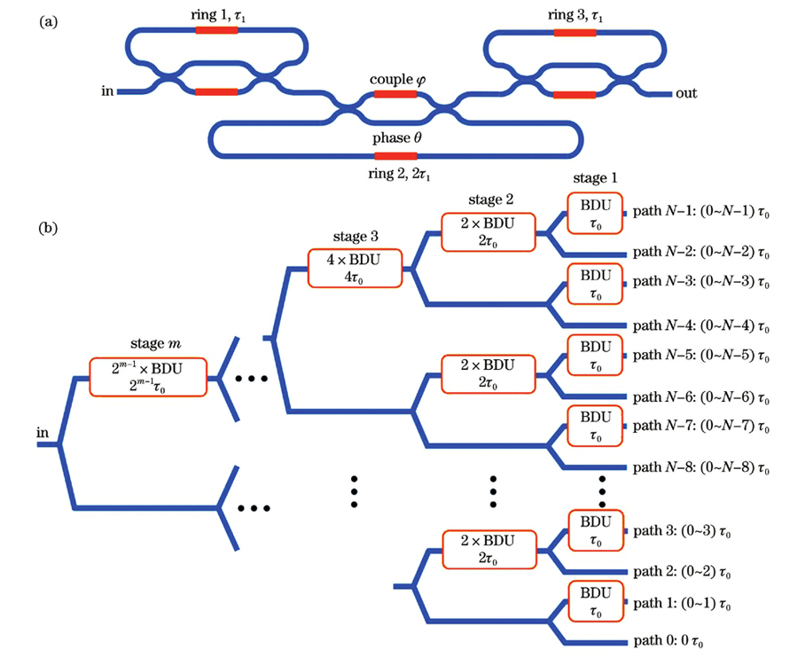
    Fig. 1. Structure of optical beamforming network (OBFN). (a) Three microring resonators (MRR) basic delay unit; (b) 1×N binary tree OBFN chip
    Simulated delay spectra of MRR at various coupling coefficients
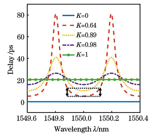
    Fig. 2. Simulated delay spectra of MRR at various coupling coefficients
    Simulated delay results of OBFN. (a) Delay spectra of the longest path in different stages of OBFNs with each BDU continuously tuned to 5 ps; (b) delay bandwidth of the longest path in different stages of OBFNs with one MRR continuously tuned in each stage
    Fig. 3. Simulated delay results of OBFN. (a) Delay spectra of the longest path in different stages of OBFNs with each BDU continuously tuned to 5 ps; (b) delay bandwidth of the longest path in different stages of OBFNs with one MRR continuously tuned in each stage
    Pictures of chip before and after packaging. (a) Microscopy image of BDU chip; (b) cross section of Si3N4 waveguide; (c) microscopy image of 1×8 OBFN chip; (b) picture of packaged chip with optical and electrical connections
    Fig. 4. Pictures of chip before and after packaging. (a) Microscopy image of BDU chip; (b) cross section of Si3N4 waveguide; (c) microscopy image of 1×8 OBFN chip; (b) picture of packaged chip with optical and electrical connections
    Schematic of experimental setup for optical and microwave measurement
    Fig. 5. Schematic of experimental setup for optical and microwave measurement
    Flowchart of optical and microwave group delay calibration
    Fig. 6. Flowchart of optical and microwave group delay calibration
    Optical calibration of MRRs. (a) Measured thermal efficiency of MRR phase shifter (MRR PS); (b) simulated transmission spectra of an MRR at various coupling coefficients; (c) MSE of optical transmission as a function of MZI PS power for K=1 state calibration; (d) measured optical transmission of a BDU at the shortest and the longest delay states
    Fig. 7. Optical calibration of MRRs. (a) Measured thermal efficiency of MRR phase shifter (MRR PS); (b) simulated transmission spectra of an MRR at various coupling coefficients; (c) MSE of optical transmission as a function of MZI PS power for K=1 state calibration; (d) measured optical transmission of a BDU at the shortest and the longest delay states
    Optical characterization for MRR resonance alignment. (a) Process of MRR resonance alignment; (b) power relationship between MZI phase shifter and microring phase shifter for resonance alignment
    Fig. 8. Optical characterization for MRR resonance alignment. (a) Process of MRR resonance alignment; (b) power relationship between MZI phase shifter and microring phase shifter for resonance alignment
    Measured delay spectra of a continuously tuned MRR at different coupling coefficients
    Fig. 9. Measured delay spectra of a continuously tuned MRR at different coupling coefficients
    Experimental results of microwave delay characterization. (a) Microwave delay spectra of optical characterization results, where MRRs are affected by thermal crosstalk; (b) measured microwave delay spectra of path 7 as MRRs are digitally tuned from K=0 state to K=1 state one by one, where MRR states are optimized to eliminate the effect of thermal crosstalk; (c) microwave delay spectra of three continuously tuned MRRs at various delay increments; (d) delay fluctuation of three continuously tuned MRRs over the frequency of 08 GHz at various delay increments
    Fig. 10. Experimental results of microwave delay characterization. (a) Microwave delay spectra of optical characterization results, where MRRs are affected by thermal crosstalk; (b) measured microwave delay spectra of path 7 as MRRs are digitally tuned from K=0 state to K=1 state one by one, where MRR states are optimized to eliminate the effect of thermal crosstalk; (c) microwave delay spectra of three continuously tuned MRRs at various delay increments; (d) delay fluctuation of three continuously tuned MRRs over the frequency of 08 GHz at various delay increments
    ContentThis workOBFN[10]OTTDL[19]OBFN[23]OTTDL[24]OBFN[31]
    Material platformSi3N4Si3N4Si3N4SOISOISi3N4
    Input×output1×81×41×11×41×11×8
    Bandwidth /GHz86.392162.5
    MRR number36845412
    Delay range /ps05608.7208.70209.43620001601801200
    Delay fluctuation /ps11.2168.5 6.2100
    Automatic calibrationYesNoNoYesNoNo
    Table 1. Comparison of several integrated OBFNs and optical true time delay lines based on cascaded MRRs
    Hanwei Sun, Liangjun Lu, Minhui Jin, Jiao Liu, Linjie Zhou, Jianping Chen. Automatic Calibration of Optical Beamforming Network Chip Based on Cascaded Anti-Resonant Microring[J]. Chinese Journal of Lasers, 2022, 49(11): 1119001
    Download Citation