
Yurou Guan, Lingling Song, Hui Zhao, Renjun Du, Liming Liu, Cuixia Yan, Jinming Cai. Two-dimensional hexagonal Zn3Si2 monolayer: Dirac cone material and Dirac half-metallic manipulation[J]. Chinese Physics B, 2020, 29(8):
- Chinese Physics B
- Vol. 29, Issue 8, (2020)
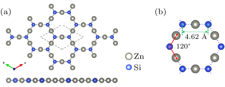
Fig. 1. (a) Optimized geometry of Zn3Si2 monolayer, with a unit cell labeled by the black dotted line. (b) A zoom-in figure of (a).
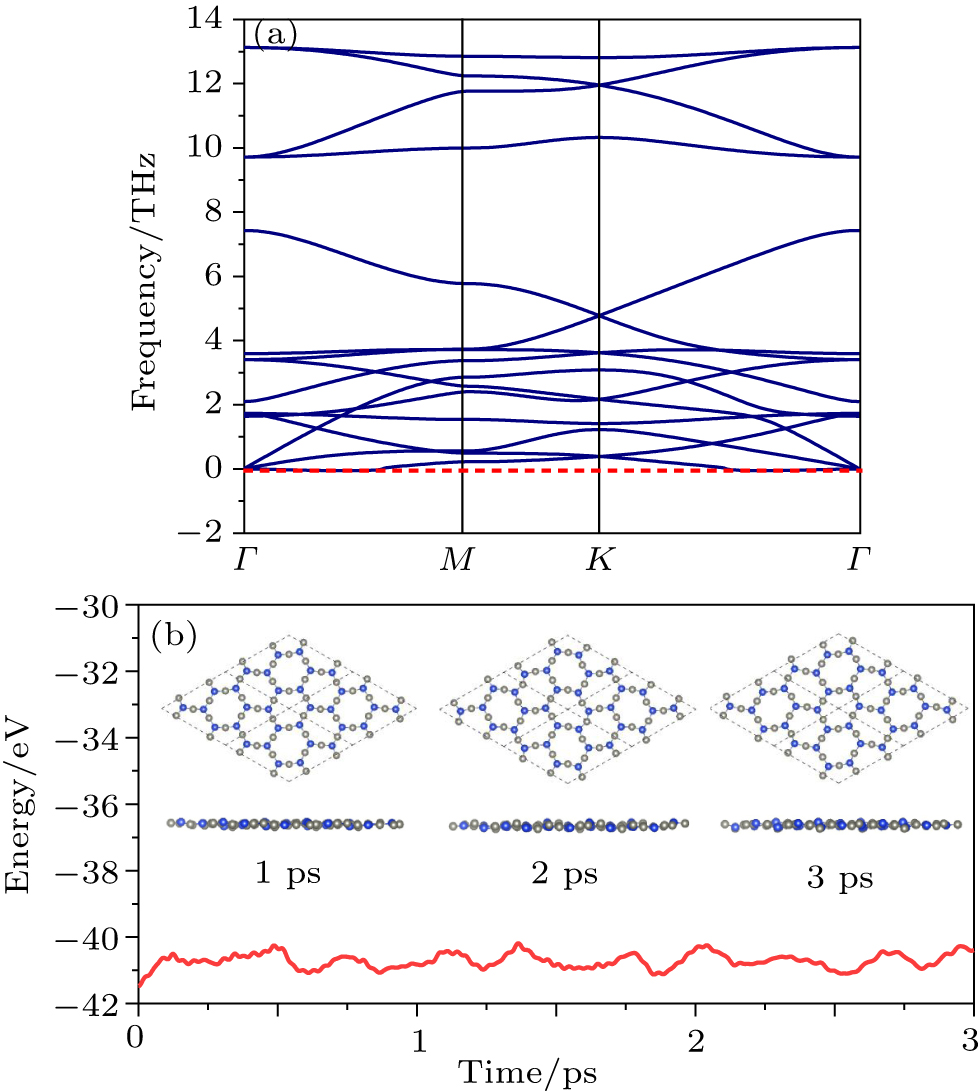
Fig. 2. (a) Phonon dispersion of Zn3Si2 monolayer, where no soft mode is found. (b) The total energy for the Zn3Si2 lattice as a function of simulation time at 300 K. The inset illustrates the snapshots of the optimized crystal structures of the Zn3Si2 lattice at 1 ps, 2 ps, and 3 ps.
Fig. 3. (a) The charge density difference with an isovalue of 0.02 e /Å−3. The blue and orange mean electron accumulation region and electron depletion region, respectively. (b) ELF of Zn3Si2 monolayer with an isovalue of 0.03 e /Å−3. (c), (d) Top and side views of VB maximum and CB minimum charge density contours at the Dirac point of Zn3Si2 monolayer, respectively.
Fig. 4. The electronic properties of Zn3Si2 without SOC. (a) The orbital-resolved band structures for Zn3Si2 monolayer (yellow: total pz orbitals; light grey: total py orbitals; blue: total px orbitals; olive: total d orbitals). The Fermi level is set to zero. (b) Projected density of states of Zn3Si2 monolayer. (c) 3D projection of Dirac cone in the vicinity of the K point.
Fig. 5. (a) The calculated band structures of Zn3Si2 monolayer with SOC. The Fermi level is set to zero. (b) The zoom-in around the Fermi level corresponding to the red dotted box in (a), where the inset indicates the first Brillouin zone.
Fig. 6. (a) The ΔE = E (spin-polarized) – E (spin-nonpolarized) with respect to carrier doping calculated in the Zn3Si2 monolayer. The negative and positive values on the horizontal ordinate are for the hole and electron dopings, respectively. (b), (c) Spin-polarized band structures in the absence of SOC with the doping concentration of 0.2 hole per atom and 0.2 electron per atom, respectively.

Set citation alerts for the article
Please enter your email address
© Copyright 2018-2021 | Chinese Laser Press. All Rights Reserved 沪ICP备15018463号-20