
Qiangqiang Guo, Jinchuan Zhang, Yixuan Zhu, Xu Gao, Quanyong Lu, Ning Zhuo, Shenqiang Zhai, Junqi Liu, Lijun Wang, Shuman Liu, Fengqi Liu, "Room-temperature continuous-wave InP-based 2.01 µm microcavity lasers in whispering-gallery modes with InGaAsSb quantum well," Chin. Opt. Lett. 21, 041405 (2023)
- Chinese Optics Letters
- Vol. 21, Issue 4, 041405 (2023)
Abstract
1. Introduction
Lasers with mid-infrared semiconductors emitting varying wavelengths between 1.55 and 3 µm have attracted much attention in spectroscopy analysis, surveillance of gas traces, lidar, and diagnosis in medicine[1–3]. This is mainly due to the high transparency atmospheric window in the range of 2–2.3 µm[4] and the strong absorption lines of many chemical molecules in the range of 2–3 µm, including nitrogen oxides and hydrocarbons. The term “eye-safe” is used to describe this place of wavelengths, wherein laser systems provide an outstanding upper hand concerning free-zone implementations when compared with standard systems operating at narrower wavelengths. Recently developed on-chip sensing by integrating lasers, sensing waveguides, and detectors on a single chip is preferred for portable sensing applications[5–10]. Microresonator-based lasers are well suited for high-density optoelectronic integration because of their small volumes and low thresholds[11,12]. In addition, the high-quality factor and small mode volume significantly enhance the light–matter interaction, resulting in low thresholds and precise resonance frequencies[13,14]. For sensing applications, continuous-wave (CW) operation is required for its short linewidth and prominent stability features. It is easily achieved in the spectral ranges of telecommunication and vision, since the density of the laser has a low threshold power in these ranges[15,16]. Previously, a particular configuration was designed for electrical isolation and combined with surface passivation to achieve room-temperature CW operation of mid/long-wave mid-infrared microcavity quantum cascade lasers[17,18]. However, a microcavity laser capable of operating in CW mode above room temperature in the 2–3 µm spectral range has yet to be demonstrated.
Several material platforms have been used for lasers that operate in ranges between 2 and 3 µm, including structures related to InP-based and GaSb-based active regions[19,20]. The type-I quantum well (QW) laser on the GaSb substrate has excellent performance, and the watt-level output has been obtained under CW operation at room temperature[20,21]. Moreover, the lasers with GaSb-based interband cascade using structures of active regions pertinent to both the type-1 and type-2 reached CW operation at room temperature with relatively lower threshold current densities at longer wavelengths[22,23]. Single-mode emission has also been achieved in a variety of ways[24]. Therefore, lasers with a GaSb base have been utilized in most of the implementations. Since electrons overlapped less, functions with hole waves, and spontaneously inefficient radiation are observed, InP-based long-wavelength lasers generally lag behind the material platform of a GaSb[25]. In recent years, advancement has taken place in engineering that designs the energy band and realizes the growth of crystals deeply, and lasers with an InP base have begun to evolve swiftly and present unique advantages. Lasers with high performance emitting longer wavelengths, 2.15 µm, by using InP substrates that have higher quality, lower cost, and larger diameters have been reported[26]. A laser having a 2.37 µm wavelength and 11 mW output power at 300 K, was presented by using a design of the triangular InAs QW[27]. Our laboratory has reported a laser with a 2.1 µm InGaAsSb QW utilizing Sb as a surfactant having a notably elevated CW output power of up to 330 mW[28]. These results represent a critical step toward the practical application of long-wavelength InP-based lasers. Moreover, InP-based lasers favor concordance with advanced equipment manufacturing operation platforms, specifically the use of embedded heterostructures to raise thermal conductivity and greatly enhance the performance of equipment. For certain applications that require complex processing techniques, such as a vertically cavitated surface that emits lasers or silicon-based combined equipment, light sources of the InP-based long wavelengths are advantageous because the material platform of the InP is monolithically amicable with several photonic combined circuits. In addition, InP substrates present raised thermal conductivity and decreased cost, which makes them more qualified for industrial production on a large scale. Therefore, we are committed to developing InP material microcavity lasers due to their inherent advantages.
In this work, a higher performance of the InP-based electrically pumped microcavity laser with lasing wavelengths over 2 µm is reported. Benefiting from the InGaAsSb QWs spotted in a typically decoupled confinement heterostructure, the device achieves a CW maximum power of over 0.36 mW at 15°C and a highest CW operating temperature of over 30°C. A stable single-mode emission is attained covering the complete dynamic extent, and the frequencies of a laser are linearly adjusted concerning the pumping current. The device maintains an immensely unidirectional laser emission with a diverging beam angle that is less than 2° in the horizontal plane. These results are critical steps in the development of mid-infrared on-chip sensing.
Sign up for Chinese Optics Letters TOC. Get the latest issue of Chinese Optics Letters delivered right to you!Sign up now
2. Design and Fabrication
The InGaAsSb multiple QW structure was grown on an n-InP substrate, using a system having equipment called LayTec EpiTT that deposes metal–organic chemical vapor to surveil the in situ growth temperature of the wafer surface. Trimethylindium, triethylgallium, arsine, and phosphine function as precursors, and hydrogen is utilized as a carrier gas. 100 bar (1 bar = 105 Pa) is picked as the pressure of the reactor concerning the growth process. A buffer layer with a 300 nm
In a whispering-gallery mode (WGM) resonator, just a fragmented portion of the pump volume along the periphery of the cavity is involved in producing photons, and the remaining merely produces heat. Concerning the intensity distribution of the WGM, a particular electrical isolation configuration is adopted and is implemented in the area with no contribution to the gain of the mode of the waveguide to reduce the entire injection current, thereby reducing the internal temperature in the active region. In addition, a horizontal dissipation channel to further reduce the operative temperature available in the active region could be provided by the design. Considering the lower threshold power compared with the quantum cascade laser, we only removed the top contact layer in the electrically isolated region by using inductively coupled plasma etching with an etching depth of 300 nm (slightly deeper than the thickness of the upper contact layer), to simplify the fabrication process and reduce the cost. The contour of the cavity was also prepared by dry etching to form steep and smooth sidewalls. Then, a 450 nm thick silicon dioxide layer was grown to passivate surface defects on the sidewalls of the cavity. A window opening in the silicon dioxide layer on top of the cavity was performed by wet etching. Ti/Au and Au/Ge/Ni/Au top and back ohmic contacts were deposited via electron beam evaporation, respectively. The devices were cleaved into squares with 500-µm sides and escalated with the epilayer side down on a diamond substrate with indium solder for efficient heat dissipation.
3. Result and Discussion
The InP-based microcavity laser was mounted on a holder containing a thermoelectric cooler to regulate the heat sink temperature. The emission properties of the device were obtained in pulsed mode and CW mode, respectively. The output power was measured by a calibrated pyroelectric power meter after the beam was collected with a lens. The spectra of the device are attained by employing a fast-scanned Fourier transform infrared spectrometer having a
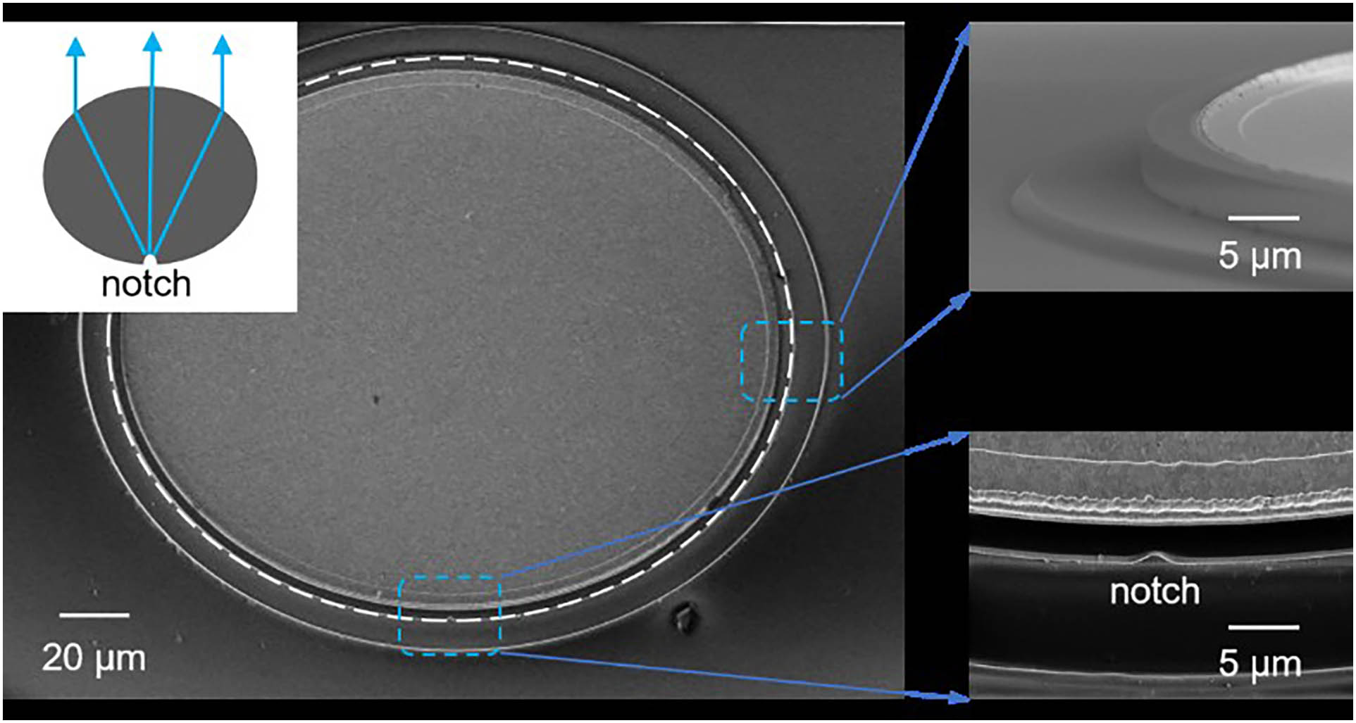
Figure 1 depicts an image of a representative scanning electron microscope utilizing a particular electrical isolation configuration, where the white line along the boundary of the cavity was drawn for eye guidance, with a semiminor
![]()
Figure 1.Scanning electron microscope image of the notched elliptical resonator. The white line is the cavity boundary. The upper left inset shows the schematic illustration of the notched elliptical resonator. The right inset shows the smooth sidewall of the laser cavity and a detail of the cavity.
Figure 2 shows the measured CW power–current-voltage attributions versus the heat sink temperature of the representative equipment. Through the optimized active region structure and efficient thermal dissipation design, the highest CW operative temperature of the InP-based microcavity laser exceeds 30°C, with a CW output power ranging from 0.36 mW at 15°C to 0.05 mW at 30°C. The threshold current of the device is about 90 mA at 15°C. Figure 3 depicts the spectra of the emitted CW as a function of the pumping current that was gathered at a fixed heat sink temperature of 15°C. The stable single-mode operation is attained in the 110–130 mA range, and the frequencies of the laser are adjusted linearly based on the pumping current with a current-tuning coefficient of
![]()
Figure 2.Measured power-current-voltage characteristics for various heat sink temperatures during CW operation.
![]()
Figure 3.CW spectra for various pumping currents at 15°C. The corresponding current tuning coefficient was −12.04 cm−1 A−1.
The in-plane far-field profile was measured under pulsed conditions at room temperature. The equipment is placed on a stage having a motorized rotation with 0.1° resolution, and a detector 40 cm away from a mercury-cadmium-telluride is used, with a maximum of 180° scan angle. As shown in Fig. 4, the device maintained a unidirectional far field, with a complete width at half-maximum beam divergence of less than 2°, which is an order of magnitude less than that of Fabry-Perot lasers with 5 µm ridge width at a similar wavelength. Combined with the stable single-mode laser action, we consider the laser mode to be an even parity mode[29].
![]()
Figure 4.Measured horizontal far-field profiles of microcavity lasers and Fabry–Perot lasers in pulsed-mode operation.
4. Conclusion
In this work, we report an InP-based high-performance electrically pumped microcavity laser with a lasing wavelength exceeding 2 µm. A maximum output power of over 0.36 mW is achieved in CW mode at 15°C, and the maximum CW operating temperature exceeds 30°C. Stable single-mode operation is attained over the complete dynamic interval, and the frequency of the laser is adjusted linearly with the pumping current. The device maintains a highly single-directional laser emission, having a less than 2° diverging angle in the horizontal plane. Besides the optimization of both active regions and high-quality QWs, these properties are also attributed to the ingenious design of the device structure. The results were a critical step for portable and highly integrated sensing applications.
References
[1] W. Lei, C. Jagadish. Lasers and photodetectors for mid-infrared 2–3 µm applications. J. Appl. Phys., 104, 091101(2008).
[2] L. S. Rothman, I. E. Gordon, A. Barbe, D. C. Benner, P. F. Bernath, M. Birk, V. Boudon, L. R. Brown, A. Campargue, J.-P. Champion, K. Chance, L. H. Coudert, V. Dana, V. M. Devi, S. Fally, J.-M. Flaud, R. R. Gamache, A. Goldman, D. Jacquemart, I. Kleiner, J. Vander Auwera. The HITRAN 2008 molecular spectroscopic database. J. Quant. Spectrosc. Radiat. Transf., 110, 533(2009).
[3] A. Bauer, K. Rößner, T. Lehnhardt, M. Kamp, S. Höfling, L. Worschech, A. Forchel. Mid-infrared semiconductor heterostructure lasers for gas sensing applications. Semicond. Sci. Technol., 26, 014032(2011).
[4] H. A. Gebbie, W. R. Harding, C. Hilsum, A. W. Pryce, V. Roberts. Atmospheric transmission in the 1 to 14 µm region. Proc. R. Soc. A, 206, 87(1951).
[5] Q. Guo, J. Zhang, K. Yang, Y. Zhu, Q. Lu, N. Zhuo, S. Zhai, J. Liu, L. Wang, S. Liu, F. Liu. Monolithically integrated mid-infrared sensor with a millimeter-scale sensing range. Opt. Express, 30, 40657(2022).
[6] B. Schwarz, P. Reininger, D. Ristanić, H. Detz, A. M. Andrews, W. Schrenk, G. Strasser. Monolithically integrated mid-infrared lab-on-a-chip using plasmonics and quantum cascade structures. Nat. Commun., 5, 4085(2014).
[7] D. Ristanic, B. Schwarz, P. Reininger, H. Detz, T. Zederbauer, A. M. Andrews, W. Schrenk, G. Strasser. Monolithically integrated mid-infrared sensor using narrow mode operation and temperature feedback. Appl. Phys. Lett., 106, 041101(2015).
[8] B. Schwarz, P. Reininger, H. Detz, T. Zederbauer, A. M. Andrews, S. Kalchmair, W. Schrenk, O. Baumgartner, H. Kosina, G. Strasser. A bi-functional quantum cascade device for same frequency lasing and detection. Appl. Phys. Lett., 101, 191109(2012).
[9] B. Schwarz, D. Ristanic, P. Reininger, T. Zederbauer, D. MacFarland, H. Detz, A. Andrews, W. Schrenk, G. Strasser. High-performance bi-functional quantum cascade laser and detector. Appl. Phys. Lett., 107, 071104(2015).
[10] B. Schwarz, C. A. Wang, L. Missaggia, T. S. Mansuripur, P. Chevalier, M. K. Connors, D. McNulty, J. Cederberg, G. Strasser, F. Capasso. Watt-level continuous-wave emission from a bifunctional quantum cascade laser/detector. ACS Photonics, 4, 1225(2017).
[11] V. S. Ilchenko, A. A. Savchenkov, A. B. Matsko, L. Maleki. Nonlinear optics and crystalline whispering gallery mode cavities. Phys. Rev. Lett., 92, 043903(2004).
[12] A. Chiasera, Y. Dumeige, P. Féron, M. Ferrari, Y. Jestin, G. Nunzi Conti, S. Pelli, S. Soria, G. C. Righini. Spherical whispering-gallery-mode microresonators. Laser Photon. Rev., 4, 457(2010).
[13] J. Faist, C. Gmachl, M. Striccoli, C. Sirtori, F. Capasso, D. L. Sivco, A. Y. Cho. Quantum cascade disk lasers. Appl. Phys. Lett., 69, 2456(1996).
[14] L. He, S. K. Ozdemir, L. Yang. Whispering gallery microcavity lasers. Laser Photonics Rev., 7, 60(2013).
[15] M. H. Mao, H. C. Chien, J. Z. Hong, C. Y. Cheng. Room-temperature low-threshold current-injection InGaAs quantum-dot microdisk lasers with single-mode emission. Opt. Express, 19, 14145(2011).
[16] I. Aharonovich, A. Woolf, K. J. Russell, T. Zhu, N. Niu, M. J. Kappers, R. A. Oliver, E. L. Hu. Low threshold, room-temperature microdisk lasers in the blue spectral range. Appl. Phys. Lett., 103, 021112(2013).
[17] Q. Guo, J. Zhang, C. Ning, N. Zhuo, S. Zhai, J. Liu, L. Wang, S. Liu, Z. Jia, F. Liu. Continuous-wave operation of microcavity quantum cascade lasers in whispering-gallery mode. ACS Photonics, 9, 1172(2022).
[18] Q. Guo, J. Zhang, R. Yin, N. Zhuo, Q. Lu, S. Zhai, J. Liu, L. Wang, S. Liu, F. Liu. Continuous-wave microcavity quantum cascade lasers in whispering-gallery modes up to 50°C. Opt. Express, 30, 22671(2022).
[19] S. Sprengel, C. Grasse, K. Vizbaras, T. Gruendl, M.-C. Amann. Up to 3 µm light emission on InP substrate using GaInAs/GaAsSb type-II quantum wells. Appl. Phys. Lett., 99, 221109(2011).
[20] A. Vizbaras, E. Dvinelis, M. Greibus, A. Trinkunas, D. Kovalenkovas, I. Šimonytė, K. Vizbaras. High-performance single-spatial mode GaSb type-I laser diodes around 2.1 µm. Proc. SPIE, 8993, 899319(2014).
[21] K. Merghem, R. Teissier, G. Aubin, A. M. Monakhov, A. Ramdane, A. N. Baranov. Passive mode locking of a GaSb-based quantum well diode laser emitting at 2.1 µm. Appl. Phys. Lett., 107, 111109(2015).
[22] I. Vurgaftman, W. W. Bewley, C. L. Canedy, C. S. Kim, M. Kim, J. Ryan Lindle, C. D. Merritt, J. Abell, J. R. Meyer. Mid-IR type-II interband cascade lasers. IEEE J. Sel. Top. Quantum Electron., 17, 1435(2011).
[23] Y. Jiang, L. Li, R. Q. Yang, J. A. Gupta, G. C. Aers, E. Dupont, J.-M. Baribeau, X. Wu, M. B. Johnson. Type-I interband cascade lasers near 3.2 µm. Appl. Phys. Lett., 106, 041117(2015).
[24] C. Ning, R. Sun, S. Liu, J. C. Zhang, N. Zhuo, J. Liu, L. Wang, S. Zhai, F. Liu, Z. G. Wang. GaSb surface grating distributed feedback interband cascade laser emitting at 3.25 µm. Opt. Express, 30, 29007(2022).
[25] D. Wang, J. Zhang, C. Hou, Y. Zhao, F. Cheng, X. Jia, S. Zhai, N. Zhuo, J. Liu, F. Liu, Z. Wang. High-performance continuous-wave InP-based 2.1 µm superluminescent diode with InGaAsSb quantum well and cavity structure suppression. Appl. Phys. Lett., 113, 161107(2018).
[26] S. Luo, H. M. Ji, F. Gao, F. Xu, X. G. Yang, P. Liang, T. Yang. High performance 2150 nm-emitting InAs/InGaAs/InP quantum well lasers grown by metalorganic vapor phase epitaxy. Opt. Express, 23, 8383(2015).
[27] Y. Gu, Y. Zhang, Y. Cao, L. Zhou, X. Chen, H. Li, S. Xi. 2.4 µm InP-based antimony-free triangular quantum well lasers in continuous-wave operation above room temperature. Appl. Phys. Express, 7, 032701(2014).
[28] D. Wang, N. Zhuo, Y. Zhao, F. Cheng, S. Niu, J. Zhang, S. Zhai, L. Wang, S. Liu, F. Liu, Z. Wang. Improved performance of InP-based 2.1 µm InGaAsSb quantum well lasers using Sb as a surfactant. Appl. Phys. Lett., 113, 251101(2018).
[29] Q. J. Wang, C. Yan, N. Yu, J. Unterhinninghofen, J. Wiersig, C. Pflügl, L. Diehl, T. Edamura, M. Yamanishi, H. Kan, F. Capasso. Whispering-gallery mode resonators for highly unidirectional laser action. Proc. Natl. Acad. Sci. U.S.A., 107, 22407(2010).


Set citation alerts for the article
Please enter your email address

© Copyright 2018-2021 | Chinese Laser Press. All Rights Reserved 沪ICP备15018463号-20