• Acta Physica Sinica
  • Vol. 69, Issue 2, 027802-1 (2020)
Cheng-Hao Gao1、2, Feng Xu2、3、*, Li Zhang2, De-Sheng Zhao2, Xing Wei2, Ling-Juan Che2, Yong-Zhang Zhuang2, Bao-Shun Zhang2、*, and Jing Zhang1、*
Author Affiliations
  • 1Institute of Optoelectronic Engineering, Changchun University of Science and Technology, Changchun 085202, China
  • 2Department of Physics, Suzhou Institute of Nano-tech and Nano-bionics, Chinese Academy of Sciences, Suzhou 215123, China
  • 3Institute of Opto-Electronic, Nanjing University & Yangzhou, Yangzhou 225009, China
  • show less
    DOI: 10.7498/aps.69.20191418 Cite this Article
    Cheng-Hao Gao, Feng Xu, Li Zhang, De-Sheng Zhao, Xing Wei, Ling-Juan Che, Yong-Zhang Zhuang, Bao-Shun Zhang, Jing Zhang. Ion implantation isolation based micro-light-emitting diode device array properties[J]. Acta Physica Sinica, 2020, 69(2): 027802-1 Copy Citation Text show less
    (a) Schematic structure of micro-LED array; (b) SEM image of 10 μm micro-LED array surface.(a) micro-LED阵列结构图; (b) 10 μm micro-LED阵列表面SEM图像
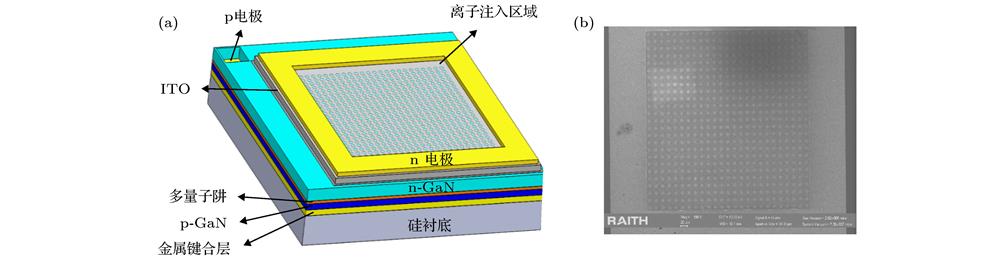
    Fig. 1. (a) Schematic structure of micro-LED array; (b) SEM image of 10 μm micro-LED array surface.(a) micro-LED阵列结构图; (b) 10 μm micro-LED阵列表面SEM图像
    (a) The I-V and (b) light output power density-current density characteristics of 6 μm arrays of samples A and B样品A和B 6 μm阵列的(a) I-V 特性和(b)光输出密度-电流密度特性
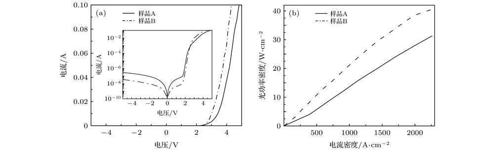
    Fig. 2. (a) The I-V and (b) light output power density-current density characteristics of 6 μm arrays of samples A and B 样品A和B 6 μm阵列的(a) I-V 特性和(b)光输出密度-电流密度特性
    Comparison of (a) reverse leakage current and (b) light output density between implanted isolated micro-LED devices and mesa etching devices.注入隔离micro-LED器件与台面刻蚀器件 (a)反向漏电流和(b)光输出密度比较
    Fig. 3. Comparison of (a) reverse leakage current and (b) light output density between implanted isolated micro-LED devices and mesa etching devices.注入隔离micro-LED器件与台面刻蚀器件 (a)反向漏电流和(b)光输出密度比较
    The relationship between damage and implantation depth of F ion with different implantation energies with SRIM simulation.SRIM模拟F离子不同注入能量下产生的损伤与注入深度关系
    Fig. 4. The relationship between damage and implantation depth of F ion with different implantation energies with SRIM simulation.SRIM模拟F离子不同注入能量下产生的损伤与注入深度关系
    Schematic of CTLM test.CTLM测量原理图
    Fig. 5. Schematic of CTLM test.CTLM测量原理图
    The CTLM linear fitting curve at (a) the implantation energy of 50 keV and (b) 50/100 keV.CTLM线性拟合曲线 (a) 50 keV能量注入; (b) 50/100 keV能量注入
    Fig. 6. The CTLM linear fitting curve at (a) the implantation energy of 50 keV and (b) 50/100 keV.CTLM线性拟合曲线 (a) 50 keV能量注入; (b) 50/100 keV能量注入
    I-V characteristics of the different emission aperture arrays.不同发光孔径阵列I-V特性曲线
    Fig. 7. I-V characteristics of the different emission aperture arrays. 不同发光孔径阵列I-V特性曲线
    Light-emitting aperture arrays of (a) 6 μm, (b) 8 μm, and (c)10 μm at 20 mA.20 mA下 (a) 6 μm, (b) 8 μm, (c) 10 μm发光孔径阵列发光图像
    Fig. 8. Light-emitting aperture arrays of (a) 6 μm, (b) 8 μm, and (c)10 μm at 20 mA.20 mA下 (a) 6 μm, (b) 8 μm, (c) 10 μm发光孔径阵列发光图像
    样品工作电压(20 mA)/V反向漏电流(–5 V)/A光输出密度(2264 A/cm–2)/W·cm–2
    A3.692.89 × 10–731.34
    B3.273.43 × 10–840.59
    Table 1.

    The photoelectric properties of 6 μm micro-LED array.

    6 μm micro-LED阵列光电性能参数

    器件尺寸/μm681020[16]10[17]
    隔离方式注入台面刻蚀
    实际发光区域
    实际发光面积S1/μm224.1043.9272.0414470 ± 10
    器件面积 S2/μm228.2650.2478.50400100
    S1/S2/% 85%87%92%36%70 ± 10
    Table 2.

    The actual emission condition of single light-emitting aperture in sample B.

    样品B单颗发光孔径实际发光情况

    Cheng-Hao Gao, Feng Xu, Li Zhang, De-Sheng Zhao, Xing Wei, Ling-Juan Che, Yong-Zhang Zhuang, Bao-Shun Zhang, Jing Zhang. Ion implantation isolation based micro-light-emitting diode device array properties[J]. Acta Physica Sinica, 2020, 69(2): 027802-1
    Download Citation