• Photonics Research
  • Vol. 8, Issue 5, 630 (2020)
Sung-Wen Huang Chen1, Yu-Ming Huang1、2, Konthoujam James Singh1, Yu-Chien Hsu1, Fang-Jyun Liou1, Jie Song3, Joowon Choi3, Po-Tsung Lee1, Chien-Chung Lin2, Zhong Chen4, Jung Han5, Tingzhu Wu4、6、*, and Hao-Chung Kuo1、7、*
Author Affiliations
  • 1Department of Photonics & Graduate Institute of Electro-Optical Engineering, College of Electrical and Computer Engineering, Taiwan Chiao Tung University, Hsinchu 30010, China
  • 2Institute of Photonic System, Taiwan Chiao Tung University, Tainan 71150, China
  • 3Saphlux Inc., Branford, Connecticut 06405, USA
  • 4Department of Electronic Science, Fujian Engineering Research Center for Solid-State Lighting, Xiamen University, Xiamen 361005, China
  • 5Department of Electrical Engineering, Yale University, New Haven, Connecticut 06520, USA
  • 6e-mail: wutingzhu@xmu.edu.cn
  • 7e-mail: hckuo@faculty.nctu.edu.tw
  • show less
    DOI: 10.1364/PRJ.388958 Cite this Article Set citation alerts
    Sung-Wen Huang Chen, Yu-Ming Huang, Konthoujam James Singh, Yu-Chien Hsu, Fang-Jyun Liou, Jie Song, Joowon Choi, Po-Tsung Lee, Chien-Chung Lin, Zhong Chen, Jung Han, Tingzhu Wu, Hao-Chung Kuo. Full-color micro-LED display with high color stability using semipolar (20-21) InGaN LEDs and quantum-dot photoresist[J]. Photonics Research, 2020, 8(5): 630 Copy Citation Text show less
    Process flow for the fabrication of a full-color RGB pixel array. (a) μ-LED array process. (b) Black PR matrices and p-electrode metal lines. (c) Red, green, and blue (transparent) pixel lithography process. (d) Color pixel bonding.
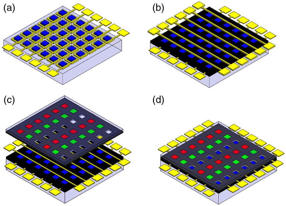
    Fig. 1. Process flow for the fabrication of a full-color RGB pixel array. (a) μ-LED array process. (b) Black PR matrices and p-electrode metal lines. (c) Red, green, and blue (transparent) pixel lithography process. (d) Color pixel bonding.
    (a) Schematic diagram of the semipolar GaN grown on a patterned sapphire substrate. (b) Photograph of a 4 in. wafer of SF-free (20-21) InGaN/GaN LED grown on a patterned sapphire substrate. (c) Top-view microscopy image of SF-free (20-21) InGaN/GaN LED grown on a patterned sapphire substrate. (d) Cross-sectional SEM image of (20-21) GaN grown on a patterned sapphire substrate by orientation-controlled epitaxy.
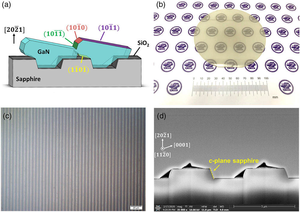
    Fig. 2. (a) Schematic diagram of the semipolar GaN grown on a patterned sapphire substrate. (b) Photograph of a 4 in. wafer of SF-free (20-21) InGaN/GaN LED grown on a patterned sapphire substrate. (c) Top-view microscopy image of SF-free (20-21) InGaN/GaN LED grown on a patterned sapphire substrate. (d) Cross-sectional SEM image of (20-21) GaN grown on a patterned sapphire substrate by orientation-controlled epitaxy.
    (a) J-V curve of semipolar μ-LEDs, with image of lighting from device. (b) Electroluminescence spectrum of semipolar μ-LED with increasing applied current density. (c) Experimental data and simulation curves for normalized external quantum efficiency of semipolar and c-plane μ-LEDs. (d) Simulated electron current density throughout whole semipolar and c-plane μ-LED structures at 20 A/cm2 and 200 A/cm2 forward current density.
    Fig. 3. (a) J-V curve of semipolar μ-LEDs, with image of lighting from device. (b) Electroluminescence spectrum of semipolar μ-LED with increasing applied current density. (c) Experimental data and simulation curves for normalized external quantum efficiency of semipolar and c-plane μ-LEDs. (d) Simulated electron current density throughout whole semipolar and c-plane μ-LED structures at 20  A/cm2 and 200  A/cm2 forward current density.
    (a) Fluorescence microscopy image of RGB pixel. (b) Overlap relationship between blue μ-LED electroluminescence emission and absorption of quantum-dot photoresist. (c) Electroluminescence spectra of red and green pixels. (d) Electroluminescence microscope image of RGB pixels.
    Fig. 4. (a) Fluorescence microscopy image of RGB pixel. (b) Overlap relationship between blue μ-LED electroluminescence emission and absorption of quantum-dot photoresist. (c) Electroluminescence spectra of red and green pixels. (d) Electroluminescence microscope image of RGB pixels.
    Peak wavelengths of c-plane and semipolar μ-LEDs in range 1 to 200 A/cm2 current density.
    Fig. 5. Peak wavelengths of c-plane and semipolar μ-LEDs in range 1 to 200  A/cm2 current density.
    Color gamut of RGB pixel assembly from c-plane μ-LED and QDPR under various current densities in (a) CIE 1931 and (b) CIE 1976. Color gamut of RGB pixel assembly from semipolar μ-LED and QDPR under various current densities in (c) CIE 1931 and (d) CIE 1976.
    Fig. 6. Color gamut of RGB pixel assembly from c-plane μ-LED and QDPR under various current densities in (a) CIE 1931 and (b) CIE 1976. Color gamut of RGB pixel assembly from semipolar μ-LED and QDPR under various current densities in (c) CIE 1931 and (d) CIE 1976.
    Sung-Wen Huang Chen, Yu-Ming Huang, Konthoujam James Singh, Yu-Chien Hsu, Fang-Jyun Liou, Jie Song, Joowon Choi, Po-Tsung Lee, Chien-Chung Lin, Zhong Chen, Jung Han, Tingzhu Wu, Hao-Chung Kuo. Full-color micro-LED display with high color stability using semipolar (20-21) InGaN LEDs and quantum-dot photoresist[J]. Photonics Research, 2020, 8(5): 630
    Download Citation