• Chinese Optics Letters
  • Vol. 18, Issue 4, 043101 (2020)
Xiaofang Xu1、*, Jingbo Li1、**, Xiaohan Yang1, Sen Pan1, and Yong Bi2
Author Affiliations
  • 1School of Mechanical Engineering, Jiangsu University, Zhenjiang 212013, China
  • 2Nanjing Astronomical Instruments Co., Ltd., Chinese Academy of Sciences, Nanjing 210000, China
  • show less
    DOI: 10.3788/COL202018.043101 Cite this Article Set citation alerts
    Xiaofang Xu, Jingbo Li, Xiaohan Yang, Sen Pan, Yong Bi. Introduction of Ag nanoparticles by picosecond LIFT to improve the photoelectric property of AZO films[J]. Chinese Optics Letters, 2020, 18(4): 043101 Copy Citation Text show less
    Relationship between the lattice temperature of the Ag film and the picosecond laser energy density, wherein the thickness of the Ag film is (a) 30 nm, (b) 50 nm, (c) 100 nm, and (d) 200 nm.
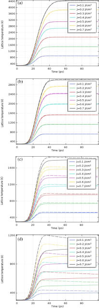
    Fig. 1. Relationship between the lattice temperature of the Ag film and the picosecond laser energy density, wherein the thickness of the Ag film is (a) 30 nm, (b) 50 nm, (c) 100 nm, and (d) 200 nm.
    Schematic diagram of the picosecond LIFT system.
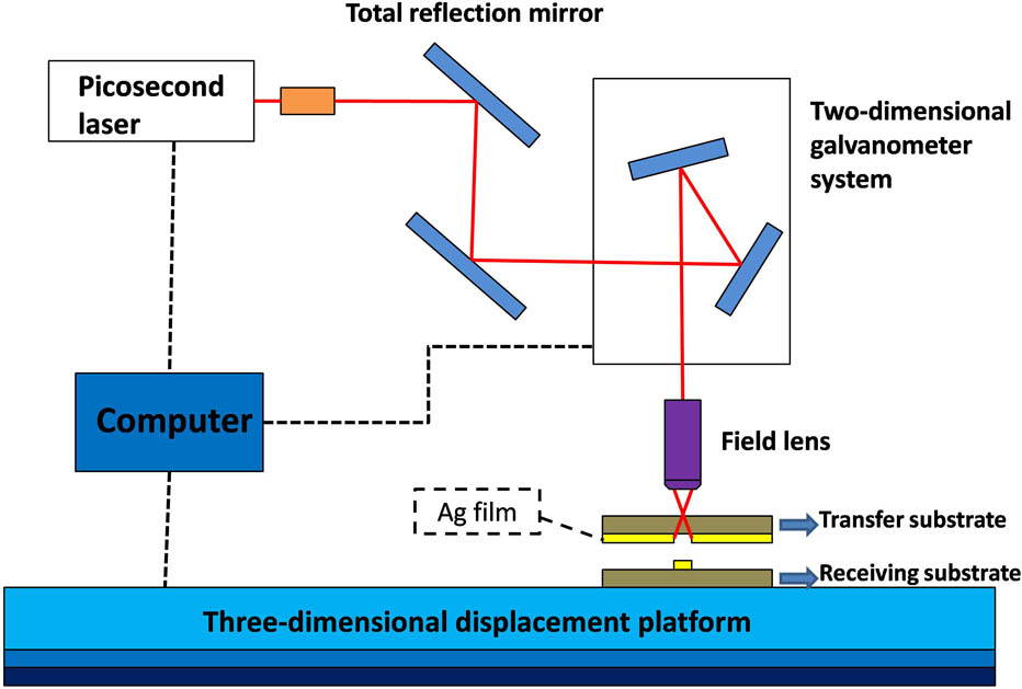
    Fig. 2. Schematic diagram of the picosecond LIFT system.
    Schematic diagram of laser scanning transfer processing. (a) Scanning pitch d=2r=30 μm. (b) Scanning pitch d=r=15 μm.
    Fig. 3. Schematic diagram of laser scanning transfer processing. (a) Scanning pitch d=2r=30μm. (b) Scanning pitch d=r=15μm.
    Micro-morphology of AZO thin film after the transfer of 50 nm Ag film under parameters E=0.79 J/cm2, v=25 mm/s: (a) 110 times, (b) 1000 times, (c) 5000 times, and (d) 17,000 times.
    Fig. 4. Micro-morphology of AZO thin film after the transfer of 50 nm Ag film under parameters E=0.79J/cm2, v=25mm/s: (a) 110 times, (b) 1000 times, (c) 5000 times, and (d) 17,000 times.
    Sectional view of Ag-AZO films after the transfer of 50 nm Ag film under parameters E=0.79 J/cm2, v=25 mm/s.
    Fig. 5. Sectional view of Ag-AZO films after the transfer of 50 nm Ag film under parameters E=0.79J/cm2, v=25mm/s.
    (a) Micro-morphology of AZO film after the transfer of a 30 nm Ag film under parameters E=0.32 J/cm2, v=15 mm/s; (b) micro-morphology of AZO thin film after the transfer of a 50 nm Ag film under parameters E=0.79 J/cm2, v=25 mm/s.
    Fig. 6. (a) Micro-morphology of AZO film after the transfer of a 30 nm Ag film under parameters E=0.32J/cm2, v=15mm/s; (b) micro-morphology of AZO thin film after the transfer of a 50 nm Ag film under parameters E=0.79J/cm2, v=25mm/s.
    (a) AFM diagram of initial AZO film; (b) AFM diagram of 30 nm Ag-AZO film.
    Fig. 7. (a) AFM diagram of initial AZO film; (b) AFM diagram of 30 nm Ag-AZO film.
    (a) Light transmittance curves of the AZO film samples after the transfer of 50 nm Ag films; (b) light transmittance curves of the AZO film samples after the transfer of 30 nm Ag films.
    Fig. 8. (a) Light transmittance curves of the AZO film samples after the transfer of 50 nm Ag films; (b) light transmittance curves of the AZO film samples after the transfer of 30 nm Ag films.
    NumberLaser ParameterTav (%)Rs(Ω/sq)FTC(×102Ω1)
    E(J/cm2)V (mm/s)
    0//79.789.198.68
    10.221565.488.607.61
    20.322061.928.147.60
    30.482061.517.977.76
    40.502060.807.917.68
    50.652070.127.898.88
    60.792575.437.879.58
    71.982058.3920.282.88
    Table 1. Experimental Parameters and Transmittance, Sheet Resistance, and Quality Factor of 50 nm Ag Film Transfer Sample
    NumberLaser ParameterTav (%)Rs(Ω/sq)FTC(×102Ω1)
    E(J/cm2)V (mm/s)
    0//78.039.118.56
    10.151574.488.458.81
    20.221571.648.428.51
    30.221574.697.939.41
    40.321568.327.918.63
    50.321569.188.108.54
    60.411570.638.018.82
    70.411569.197.858.81
    Table 2. Experimental Parameters and Transmittance, Sheet Resistance, and Quality Factor of 30 nm Ag Film Transfer Sample
    Number0123
    Roughness (nm)3.64917.59620.36721.485
    Table 3. Surface Roughness of AZO Film after 30 nm Ag Film Transfer
    Xiaofang Xu, Jingbo Li, Xiaohan Yang, Sen Pan, Yong Bi. Introduction of Ag nanoparticles by picosecond LIFT to improve the photoelectric property of AZO films[J]. Chinese Optics Letters, 2020, 18(4): 043101
    Download Citation