Abstract
Titanium nitride (TiN) as a refractory plasmonic material is proposed to be used as an angle-insensitive integrated broadband solar absorber and narrowband near-infrared (NIR) emitter for solar thermo-photovoltaic (STPV) application. By constructing TiN-nanopatterns/dielectric/TiN stack metamaterial, approximately 93% light absorption in a wavelength range of 0.3–0.9 μm and near unit narrowband (Δλ∕λ ~ 0.3) emission in NIR (~2 μm) were demonstrated by numerical simulation. Keeping the excellent light absorption in the visible band, the emission wavelength can be easily tuned by patterning the top TiN layer into various subwavelength structures. This dual function attributes to the intrinsic absorption and plasmonic property of TiN. In such an integrated structure, broadband absorption and narrowband emission need to be balanced for an optimized power efficiency conversion. Detailed analysis has demonstrated that the STPV system based on this integrated absorber/emitter can exceed the Shockley–Queisser limit at 1000 K.1. INTRODUCTION
Photovoltaics (PV) is a common method to convert solar energy into electricity. Significant effort has been put in to improve the performance and cut down the price. However, the power conversion efficiency (PCE) of single-junction PV cells is subject to the Shockley–Queisser (SQ) limit [1], which stems from a mismatch between the incident photon energy and the bandgap of the solar active material, resulting in thermal loss. Generally, it includes: (1) photons with the energy below the bandgap of the solar cell cannot be absorbed; (2) photons with the energy above the bandgap lose their extra energy as undesirable thermalization. Therefore, a crystalline silicon solar cell has a limited PCE of 30% [2]. Compared with a typical PV device, the solar thermo-photovoltaic (STPV) conversion system is considered capable of breaking the SQ limit, where the solar energy is absorbed by the STPV absorber, and then the thermal emitter radiates in a narrowband that matches with the bandgap of the solar cell. As a result, the above-mentioned two thermal loss are suppressed [3,4]. Furthermore, roughly 50% of energy involved in conventional energy conversion processes, based on oil and coal, eventually dissipates as waste heat [5]. These thermal loss also can be utilized as a heat resource and converted into usable electric power by STPV application.
Commonly, the STPV system consists of an absorber, a thermal emitter, and solar cell, where the absorber absorbs and transfers the solar energy to the emitter following with the thermal radiation from the emitter toward the solar cell. Broadband high-efficiency absorption of the absorber and narrowband emission of the emitter matching with the bandgap of the solar cell are desired to achieve a high PCE. A blackbody is an ideal absorber, which absorbs all radiation incident upon it. According to Kirchoff’s law of thermal radiation, the emissivity of a material equals its absorptivity at every wavelength point at equilibrium temperature. Consequently, an ideal absorber is typically not a good emitter. Because the photon density and the thermal radiation can be engineered by photonic crystals, the absorption and emission can be modified in these structures. It has been demonstrated that 1D dielectric photonic crystal structures are successfully integrated into millimeter-scale STPV systems and experimentally achieve a higher efficiency of 2.5% than a graybody emitter under the same energy inputs [6]. Thus far, most STPV structures are designed based on the separated absorber and emitter [7–9], where heat storage in the absorber will be transferred to the emitter through heat conduction. Unfortunately, thermal resistance between absorber and emitter inescapably leads to energy loss and ultimately reduces the overall efficiency of the STPV system. By integrating the multiwalled carbon nanowire absorber and multilayer emitter on the same thermally conducting silicon substrate, a record efficiency of 3.2% is experimentally obtained due to the reduced thermal conduction loss between the absorber and emitter [10]. However, the -stack-based 1D photonic crystal emitters are vulnerable to degradation at high temperature and angle sensitive. To further suppress the thermal conduction loss, a combined absorber and emitter is preferred. Therefore, spectral engineering for high-efficiency broadband absorption and narrowband emission in the same structure is one of the most important topics in STPV. Metallic materials with intrinsic light absorption in the visible range and spectral engineering capability provide an alternative method to construct integrated STPV absorber/emitter. Metallic nanostructures have already demonstrated light trapping and spectral engineering capabilities in the PV application [11–21]. The broadband absorption enhancement mechanisms are based on plasmonic and metamaterial photonics, where light transmission behavior could be manipulated by tuning the size and shape of the nanostructure and the properties of the medium. Metamaterial-based perfect absorbers with angle independence have already been demonstrated in various frequency bands with a tunable narrowband emission [14,15]. Polarization independent absorption above 71% in a broadband between 0.4 and 0.7 μm is demonstrated and indicates further improvement to 85% [22]. Although the main obstacle in straight utilization of plasmonic-enhanced absorption in the PV system is significant Ohmic loss, the induced temperature rise in a confined volume around the nanostructure shows great potential for a high PCE in STPV system. However, the commonly used plasmonic/metamaterial materials are noble metals, which have relatively low melting points; for example, silver (Ag) and gold (Au) have a melting point of 961°C and 1063°C, respectively [8]. Furthermore, the melting point quickly drops when the metal is patterned into the nanometer scale [23]. On the other hand, the broadband light absorption in the STPV system inevitably leads to high operational temperature, estimated up to 1000°C, which is important to enhance the overall PCE. Therefore, noble metal-based spectral engineering structures cannot be used in the STPV system. As a result, high lossy refractory metals such as tantalum (Ta), molybdenum (Mo), and tungsten (W) have been proposed as absorbers and emitters [8,24–26]. However, the refractory metal-based nanostructures have weak spectral engineering capability and are difficult for obtaining narrowband emission [25]. Furthermore, even with protective layers made of refractory dielectric materials (hafnium dioxide) the tungsten-based photonic structure collapses at temperatures above 1400°C [27].
Recently, it has been reported that the titanium nitride (TiN) exhibits a plasmonic resonance in the visible and near-infrared (NIR) wavelength [28,29]. The imaginary part of the complex refraction index is large [30]. Additionally, it is refractory (melting point as high as 2900°C), stable, and hard (used for coating) [28,29,31]. Compared with noble metal-based coatings, TiN-based multilayer structures have superior thermal and chemical stability. In addition, unlike metals with untunable optical properties, TiN as a nonstoichiometric ceramic material has optical properties depending greatly on deposition temperature, substrate, flow ratio in the manufacturing chamber, and many other fabrication parameters [29]. As a result, TiN has the potential to optimize its optical properties according to the desired application and performance.
Sign up for Photonics Research TOC. Get the latest issue of Photonics Research delivered right to you!Sign up now
In this paper, we propose a TiN-nanopatterns/dielectric/TiN metamaterial as a combiner of broadband absorber and narrowband thermal emitter (BANE). Approximately 93% broadband light absorption in a range of 0.3–0.9 μm and near unit narrowband () tunable emission in NIR was demonstrated by numerical simulation. The mechanisms of enhanced absorption and engineered emission in TiN metamaterial are discussed, and the balance of absorption and emission is investigated in this integrated absorber and emitter structure for STPV application. Finally, the PCE of the STPV system based on TiN BANE structure is evaluated in detail.
2. BANE STRUCTURE
The BANE structure consists of TiN nanopatterns/AlN/TiN stack, as shown in Fig. 1. Considering the polarization independence and reliable fabrication, in-plane symmetrical crosses are considered in this paper. Compared with squares or spheres, the proposed cross-based metamaterial shows higher absorption in visible and easily tunable NIR resonance. In addition, crosses have shown angular robust spectral response [32]. Due to the metal-like property of TiN, this stack is similar to the well-developed metal-insulator-metal metamaterial absorbers, whose electromagnetic response could be tuned [33]. High-efficiency solar energy absorption is obtained by suppression of transmission and reflection loss, which is realized by TiN reflector (0.1 μm film) and impedance-matching TiN nanostructure. The middle dielectric layer is AlN with a high melting point up to 2200°C. The total thickness of the BANE structure is no more than two hundreds nanometers, so that it could be wrapped upon various thermal source structures. In addition, owing to the increased surface-to-volume ratio, this thin film can be easily heated and reduce the mechanical load of the system, thus enabling high-temperature durability. When it is exposed to the sunlight, the absorbed light is converted to thermal energy in the BANE structure, resulting in rise of temperature. Then, its thermal emission is converted to electricity by the solar cell. To achieve a high PCE, efficient light absorption and narrowband emission matching the bandgap of solar cell are the two key factors.
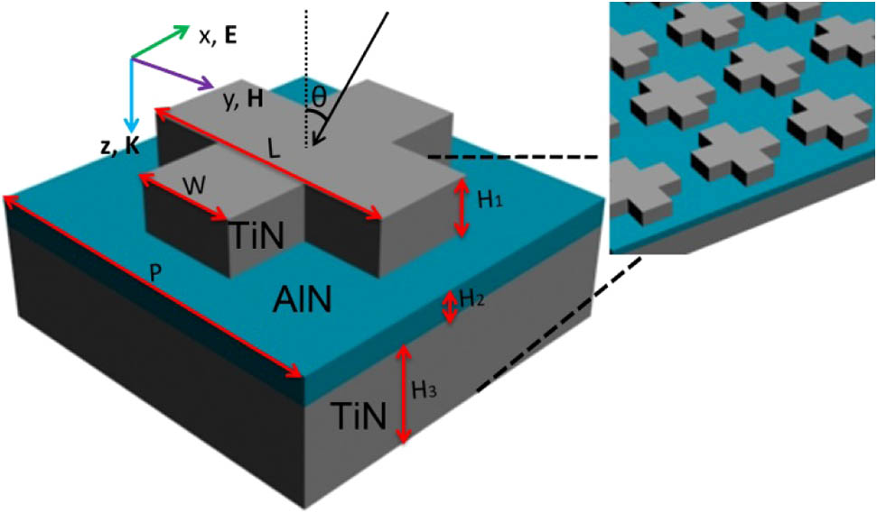
Figure 1.Schematic of the BANE structure and the geometric parameters of one unit cell. The BANE film is a three-layered structure consisting of lossy TiN cross features on top of a lossless AlN layer and a substrate of TiN.
A Lumerical FDTD solution was used to evaluate the performance of the BANE structure. An optical constant of TiN is taken from [30], and the refractive index of lossless AlN is taken from the reflective index database [34]. Nonuniform meshes were chosen with a minimum mesh size of 2 nm. The normalized absorption spectra of the BANE structure are plotted in Fig. 2(a). At the normal incidence, the BANE structure shows a high average absorption of 93% in a wavelength range of 0.3–0.9 μm, which contains 90% energy of solar radiation. This absorption is due to the intrinsic material loss of TiN in the high-frequency range, which then converts to thermal energy. In addition, there is an absorption peak close to 2 μm with near unit absorption. The FWHM is 0.66 μm, resulting in a narrow absorption band . In contrast, the blackbody emission spectrum at 1500 K peaked at 2 μm has a FWHM of 2.4 μm. Different from that in the visible range, it is a resonant absorption due to the plasmonic effect in the metamaterial BANE structure. Although it has little effect on the whole solar energy absorption, it plays an important role in thermal emission. As seen in Fig. 2(a), angular independence of the absorption spectrum is shown up to 40°, which is desirable for solar radiation absorption and thermal emission. This improved acceptance angle for high absorption eliminates the need for mechanical tracking of a STPV system, which can have a substantial impact on the first cost as well as the operating and maintenance costs. According to Kirchoff’s law of thermal radiation, the thermal emission spectrum, , of the BANE structure is the product of its absorption spectrum and the blackbody radiation spectrum: where is the ideal blackbody emission spectrum at absolute temperature , and is the polarization- and angle-averaged emission spectrum of the BANE structure. Considering the energy conversion process in a solar cell, the mismatch between its bandgap and the emitter thermal radiation limits the PCE and poses a threat to the stability of the converter system. Therefore, we can achieve efficient energy conversion if the NIR absorption peak matches the blackbody radiation peak and the bandgap of the solar cell. The relatively narrowband reduces the thermal loss usually existing in a PV system. As shown in Fig. 2(b), although the blackbody radiation is broadband, the thermal emission of the BANE structure is limited in a relatively narrowband. Especially at an optimal temperature of 1500 K, the emission bandwidth is only one fourth that of the blackbody. At a lower (higher) temperature, the peak of blackbody radiation has a red (blue) shift, and the resulting mismatch leads to a broadened emission spectrum. For example, at 2000 K, an extra emission peak around 0.8 μm is observed due to the overlap between the visible band absorption and the blackbody radiation, leading to thermalization loss.

Figure 2.(a) Polarization-averaged normalized absorption spectra of a BANE structure: ; ; ; ; ; for various incidence angles. (b) Radiation spectra of blackbody and the BANE structure at 800, 1500, and 2000 K. (c) Normalized absorption spectra for varying of 0.24, 0.26, 0.28, 0.3, and 0.32 μm. Normalized absorption spectrum as a function of width of cross structure ( in Fig. 1) in (d) and height of cross structure ( in Fig. 1) in (e). (f) Normalized reflection (black line) transmission (red line) and absorption (blue line) spectra of 0.1 μm TiN film.
To date, to harvest solar radiation, most BANE structures aim at a broad absorption band in visible and NIR range [25], but few works have considered the influence of broadband absorption to the emission. A balance of the energy absorption and the narrowband emission should be considered in the BANE design, as discussed below. In addition, as shown in Fig. 2(c), the absorption peak of the BANE structure can be easily tuned in the NIR range by varying , while the unit absorption and the narrowband emission peak are maintained. This tunability of the BANE structure provides an easy match to the bandgap of the solar cell and the blackbody radiation at different temperature, which can dramatically improve the performance of the STPV system [8,35]. Compared with Fig. 2(c), the width and height of the cross structure have less influence on the absorption spectrum, as shown in Figs. 2(d) and 2(e), respectively. Other parameters such as and also have this size-insensitive property, which can ensure a stable performance even considering that the dimension error usually appears in experimental progress. Figure 2(f) shows the transmission, reflection, and absorption spectrum of 0.1 μm TiN film. Significant absorption can be seen in the visible band considering the ultrathin film. This indicates that the broadband high absorption of the BANE structure attributes to the material intrinsic property. In contrast, flat and high reflection from 0.8 μm to longer wavelength means that the NIR absorption peak, shown in Fig. 2(a), is due to the BANE structure. Distributions of the electric field () in the plane and the magnetic field () in plane for TE polarization at the resonance wavelength of 2 μm are plotted in Figs. 3(a) and 3(b), respectively. As seen, the resonant fields are strongly confined within the insulator film, thus depicting a typical feature of cavity resonance [36,37]. Comparatively, the electric [in Fig. 3(c)] and magnetic field distributions [in Fig. 3(d)] at nonresonance wavelength of 1.25 μm are much weaker, indicating a greatly reduced resonance and light absorption. As shown in Fig. 2, by tuning the structure dimensions, the plasmonic resonance wavelength can be changed. Therefore, plasmonic modes play an important role in a controllable narrowband NIR emission-matching PV cell in the STPV system.
Figure 3.(a) Field distributions. (b) Resonance wavelength of 2 μm. (c), (d) Nonresonance wavelength of 1.25 μm for the BANE structure in Fig. 2(a) at normal incidence. (a) and (c) Electric field. (b) and (d) Magnetic field.
3. STPV SYSTEM BASED ON THE BANE STRUCTURE
For the STPV system, the overall efficiency is determined by the absorber efficiency and the solar cell efficiency . The absorber efficiency can be defined as the ratio between the power absorbed by the BANE structure and the incident solar energy [25]: where is the solar temperature, is the concentrations of the Sun, is the solid angle, is incident angle, is the absorption spectrum, and is the blackbody radiation at following Planck’s law: where is the Planck constant, is the speed of light, is the Boltzmann constant, and is the absolute temperature of the blackbody. Based on the calculated absorption spectra in Section 2, the calculated is 85%.
The solar cell efficiency consists three parts [8,25]: The first part in Eq. (4) is the ultimate efficiency, i.e., the maximum heat to electricity conversion efficiency: In the equation, the denominator is all the energy radiated from the emitter at temperature , which is calculated by the integral of blackbody radiation multiplying emissivity of the emitter at all emitting angles. The numerator is the total energy contained in the excited electron–hole pairs, where each photon with energy higher than (bandgap of the active material in the solar cell) generates one electron–hole pair. The calculation indicates that all the photons with energy above will excite one electron–hole pair, which is affirmatively delivered to the external circuit. It assumes that the photons with energy above not absorbed by the solar cell will be returned to the absorber and reabsorbed, and the recombination of the excited electron–hole pairs mostly through radiative instead of nonradiative processes. Practically, the loss in material is high; hence, efficiency of solar cell system is lower. First, not all the excited electron–hole pairs contribute to the external current. This effect is considered by the second part of Eq. (4), i.e., the recombination efficiency . It can be measured as the ratio of the open-circuit voltage to the initial material bandgap voltage [8,38], where is the charge of one electron: where is the voltage of the solar cell determined by solar cell temperature , describes nonideal factors of the solar cell such as nonradiative recombination and nonunit absorption of the incident photons and is chosen as 0.5 for an ideal case [8]: is the photon fluxes incident on the solar cell from emitter at the temperature ; is the photon fluxes incident on the solar cell from an ideal blackbody surrounding the solar cell at the temperature . Second, the third part in Eq. (4), the impedance matching factor, is utilized to evaluate the real performance of the STPV system when the operating voltage is employed to maximize the electrical power for the solar cell [8,25]: where and is related to :
By solving Eqs. (2)–(10), each efficiency factor in Eq. (4), , , and , is calculated as a function of the bandgap and the temperature of the emitter . The absorption spectra at every incidence angle also determine the rollover efficiency.
In the integral absorber and emitter structure, we need to note that the high absorption in the visible and NIR range means emission as well, where the emitting photons have much higher energy than of the solar cell, therefore causing thermalization loss. A balance between the broadband absorption and the narrowband emission should be considered in the BANE design: is an artificial absorption/emission spectrum, as shown in Fig. 4(a), which is applied to investigate this effect.
Figure 4.(a) Artificial absorption/emission spectrum . (b) Maximum overall PCE as a function of and .
Figure 5.Contours of (a) ultimate efficiency, , (b) recombination efficiency, , (c) impedance matching factor, , (d) overall STPV efficiency, .
Because we focus on the bandwidths, this spectrum is set to have two unit absorption/emission bands separated by one 10% absorption/emission band, which enables us to analyze the bandwidth effects. A large means broadband absorption in the visible and NIR range. A small describes a narrowband in the thermal emission; is the distance between these two bands. Varying , , , a series of spectra are obtained. As shown in Fig. 4(b), if we set , the highest PCE as a function of and can be obtained. At a fixed , a small shows a low overall PCE due to the reduced light absorption. By contrast, an increasing also reduces the overall PCE. This is because the increase of , i.e., a decrease of , causes dual-peak emission as shown in Fig. 2(b). The broaden emission substantially emits photons with energy far beyond , thus causing thermal loss, as shown in Eq. (5). This significant thermal loss even surpasses the extra absorption by the broadened absorption band. Therefore, we have to balance the broad visible/NIR absorption and narrowband NIR emission. The maximum PCE of 54% is observed at and for optimized and . For the spectrum of a practical device, as plotted in Fig. 2(a), the calculation results are presented in Fig. 5. As shown in Fig. 5(a), the optimal ultimate efficiency of the STPV system is yielded slightly below , corresponding to the emission peak. This indicates that the overall efficiency is enhanced by the BANE structure through minimizing the number of trivial thermal photons with energies below the bandgap energy. The maximum ultimate efficiency of 0.65 is achieved at a modest temperature of 1500 K. The mismatch between the emission peak and the blackbody radiation spectrum at higher and lower temperature attenuates the efficiency in these two ranges, whereas optimal overall efficiency above 0.36 is gained at a higher temperature of 1900 K, as shown in Fig. 5(d), which is due to the monotonic increase of and in Eq. (4), as shown in Figs. 5(b) and 5(c), respectively. At a temperature as low as 1000 K, the overall efficiency still exceeds the SQ limit [1]. Considering the size-insensitive property previously discussed, the performance of the BANE structure is stable even under nonperfect conditions. In addition, there is a localized maximum of PCE in the top right corner, i.e., high temperature region, of Figs. 5(a) and 5(d), which attributes to the influence of high absorption (i.e., another emission peak) in 0.3–0.9 μm illustrated in Fig. 2(c). In this condition, the main emission peak is located in the visible range. Therefore, in this integrated absorber and emitter configuration, we have to consider the balance between the broadband absorption and efficient emission.
4. CONCLUSIONS
A metamaterial structure based on TiN-nanopatterns/AlN/TiN stack is proposed and numerically investigated as an integrated absorber and emitter for application in the STPV system. The refractory material TiN offers broadband high-efficiency solar absorption and narrowband thermal emission. The plasmonic metal-like properties of TiN metamaterial show a tunable spectral engineering function and angle-insensitive absorption/emission, which are desirable for STPV. With a balance between the broadband absorption and narrowband emission, operating beyond the SQ limit is predicted at a temperature as low as 1000 K. These results show promising application of TiN in a STPV system.
Acknowledgment
Acknowledgment. This work is supported by grants from the National Natural Science Foundation of China (Nos. 11274344 and 61574158), the Suzhou Science and Technology Development Program Foundation (No. ZXG201425), and the general financial grant from the China Postdoctoral Science Foundation (No. 2014M560457).
References
[1] W. Shockley, H. J. Queisser. Detailed balance limit of efficiency of p-n junction solar cells. J. Appl. Phys., 32, 510-519(1961).
[2] M. A. Green, K. Emery, Y. Hishikawa, W. Warta, E. D. Dunlop. Solar cell efficiency tables (Version 45). Prog. Photovoltaics, 23, 1-9(2015).
[3] W. Spirkl, H. Ries. Solar thermophotovoltaics: an assessment. J. Appl. Phys., 57, 4409-4414(1985).
[4] T. J. Coutts. A review of progress in thermophotovoltaic generation of electricity. Renew. Sustain. Energ. Rev., 3, 77-184(1999).
[5] U. Buskies. The efficiency of coal-fired combined-cycle powerplants. Appl. Therm. Eng., 16, 959-974(1996).
[6] W. R. Chan, P. Bermel, R. C. N. Pilawa-Podgurski, C. H. Marton, K. F. Jensen, J. J. Senkevich, J. D. Joannopoulos, M. Soljacic, I. Celanovic. Toward high-energy-density, high-efficiency, and moderate-temperature chip-scale thermophotovoltaics. Proc. Natl. Acad. Sci. USA, 110, 5309-5314(2013).
[7] E. Rephaeli, S. Fan. Tungsten black absorber for solar light with wide angular operation range. Appl. Phys. Lett., 92, 211107(2008).
[8] E. Rephaeli, S. Fan. Absorber and emitter for solar thermo-photovoltaic systems to achieve efficiency exceeding the Shockley-Queisser limit. Opt. Express, 17, 15145-15159(2009).
[9] H. Tao, N. I. Landy, C. M. Bingham, X. Zhang, R. D. Averitt, W. J. Padilla. A metamaterial absorber for the terahertz regime: design, fabrication and characterization. Opt. Express, 16, 7181-7188(2008).
[10] A. Lenert, D. M. Bierman, Y. Nam, W. R. Chan, I. Celanovic, M. Soljacic, E. N. Wang. A nanophotonic solar thermophotovoltaic device. Nat. Nanotechnol., 9, 126-130(2014).
[11] Y. X. Cui, K. H. Fung, J. Xu, H. J. Ma, Y. Jin, S. L. He, N. X. Fang. Ultrabroadband light absorption by a sawtooth anisotropic metamaterial slab. Nano Lett., 12, 1443-1447(2012).
[12] Y. Cui, J. Xu, K. H. Fung, Y. Jin, A. Kumar, S. He, N. X. Fang. A thin film broadband absorber based on multi-sized nanoantennas. Appl. Phys. Lett., 99, 253101(2011).
[13] K. B. Alici, A. B. Turhan, C. M. Soukoulis, E. Ozbay. Optically thin composite resonant absorber at the near-infrared band: a polarization independent and spectrally broadband configuration. Opt. Express, 19, 14260-14267(2011).
[14] S. Molesky, C. J. Dewalt, Z. Jacob. High temperature epsilon-near-zero and epsilon-near-pole metamaterial emitters for thermophotovoltaics. Opt. Express, 21, A96-A110(2013).
[15] X. L. Liu, T. Tyler, T. Starr, A. F. Starr, N. M. Jokerst, W. J. Padilla. Taming the blackbody with infrared metamaterials as selective thermal emitters. Phys. Rev. Lett., 107, 045901(2011).
[16] L. Wen, F. H. Sun, Q. Chen. Cascading metallic gratings for broadband absorption enhancement in ultrathin plasmonic solar cells. Appl. Phys. Lett., 104, 151106(2014).
[17] L. Wen, Q. Chen, F. Sun, S. Song, L. Jin, Y. Yu. Theoretical design of multi-colored semi-transparent organic solar cells with both efficient color filtering and light harvesting. Sci. Rep., 4, 7036(2014).
[18] R. A. Pala, J. White, E. Barnard, J. Liu, M. L. Brongersma. Design of plasmonic thin-film solar cells with broadband absorption enhancements. Adv. Mater., 21, 3504-3509(2009).
[19] V. E. Ferry, M. A. Verschuuren, H. B. Li, E. Verhagen, R. J. Walters, R. E. Schropp, H. A. Atwater, A. Polman. Light trapping in ultrathin plasmonic solar cells. Opt. Express, 18, A237-A245(2010).
[20] C. Wu, G. Shvets. Design of metamaterial surfaces with broadband absorbance. Opt. Lett., 37, 308-310(2012).
[21] B. Jia, X. Chen, J. K. Saha, Q. Qiao, Y. Wang, Z. Shi, M. Gu. Concept to devices: from plasmonic light trapping to upscaled plasmonic solar modules. Photon. Res., 1, 22-27(2013).
[22] K. Aydin, V. E. Ferry, R. M. Briggs, H. A. Atwater. Broadband polarization-independent resonant light absorption using ultrathin plasmonic super absorbers. Nat. Commun., 2, 517(2011).
[23] Q. Jiang, S. Zhang, M. Zhao. Size-dependent melting point of noble metals. Mater. Chem. Phys., 82, 225-227(2003).
[24] V. Rinnerbauer, A. Lenert, D. M. Bierman, Y. X. Yeng, W. R. Chan, R. D. Geil, J. J. Senkevich, J. D. Joannopoulos, E. N. Wang, M. Soljačić. Metallic photonic crystal absorber-emitter for efficient spectral control in high-temperature solar thermophotovoltaics. Adv. Energy Mater., 4, 1400334(2014).
[25] C. H. Wu, B. Neuner, J. John, A. Milder, B. Zollars, S. Savoy, G. Shvets. Metamaterial-based integrated plasmonic absorber/emitter for solar thermo-photovoltaic systems. J. Opt., 14, 024005(2012).
[26] J. Fleming, S. Lin, I. El-Kady, R. Biswas, K. Ho. All-metallic three-dimensional photonic crystals with a large infrared bandgap. Nature, 417, 52-55(2002).
[27] K. A. Arpin, M. D. Losego, A. N. Cloud, H. Ning, J. Mallek, N. P. Sergeant, L. Zhu, Z. Yu, B. Kalanyan, G. N. Parsons. Three-dimensional self-assembled photonic crystals with high temperature stability for thermal emission modification. Nat. Commun., 4, 2630(2013).
[28] G. V. Naik, J. Kim, A. Boltasseva. Oxides and nitrides as alternative plasmonic materials in the optical range. Opt. Mater. Express, 1, 1090-1099(2011).
[29] G. V. Naik, J. L. Schroeder, X. Ni, A. V. Kildishev, T. D. Sands, A. Boltasseva. Titanium nitride as a plasmonic material for visible and near-infrared wavelengths. Opt. Mater. Express, 2, 478-489(2012).
[30] G. V. Naik, V. M. Shalaev, A. Boltasseva. Alternative plasmonic materials: beyond gold and silver. Adv. Mater., 25, 3264-3294(2013).
[31] M. Cortie, J. Giddings, A. Dowd. Optical properties and plasmon resonances of titanium nitride nanostructures. Nanotechnology, 21, 115201(2010).
[32] Y. Yu, Q. Chen, L. Wen, X. Hu, H.-F. Zhang. Spatial optical crosstalk in CMOS image sensors integrated with plasmonic color filters. Opt. Express, 23, 21994-22003(2015).
[33] D. F. DeMeo, N. Pfeister, C. M. Shemelya, T. Vandervelde. Metamaterial selective emitters for photodiodes. Proc. SPIE, 8982, 89820J(2014).
[34]
[35] N. P. Harder, P. Wurfel. Theoretical limits of thermophotovoltaic solar energy conversion. Semicond. Sci. Technol., 18, S151-S157(2003).
[36] M. Albooyeh, C. R. Simovski. Huge local field enhancement in perfect plasmonic absorbers. Opt. Express, 20, 21888-21895(2012).
[37] S. Akhavan, K. Gungor, E. Mutlugun, H. V. Demir. Plasmonic light-sensitive skins of nanocrystal monolayers. Nanotechnology, 24, 155201(2013).
[38] H. X. Deng, T. C. Wang, J. Gao, X. D. Yang. Metamaterial thermal emitters based on nanowire cavities for high-efficiency thermophotovoltaics. J. Opt., 16, 035102(2014).

