Yong-Hoon Lee, Honghwi Park, Inbo Kim, Sang-Jun Park, Sunghwan Rim, Byoung Jun Park, Moohyuk Kim, Yushin Kim, Myung-Ki Kim, Won Seok Han, Hosung Kim, Hongsik Park, Muhan Choi, "Shape-tailored whispering gallery microcavity lasers designed by transformation optics," Photonics Res. 11, A35 (2023)
Copy Citation Text
Semiconductor microdisk lasers have great potential as low-threshold, high-speed, and small-form-factor light sources required for photonic integrated circuits because of their high- factors associated with long-lived whispering gallery modes (WGMs). Despite these advantages, the rotational symmetry of the disk shape restricts practical applications of the photonic devices because of their isotropic emission, which lacks directionality in far-field emission and difficulty in free-space out coupling. To overcome this problem, deformation of the disk cavity has been mainly attempted. However, the approach cannot avoid significant degradation owing to the broken rotational symmetry. Here, we first report a deformed shape microcavity laser based on transformation optics, which exploits WGMs free from degradation. The deformed cavity laser was realized by a spatially varying distribution of deep-sub-wavelength-scale (60 nm diameter) nanoholes in an InGaAsP-based multi-quantum-well heterostructure. The lasing threshold of our laser is one-third of that of the same shaped homogeneous laser and quite similar to that of a homogeneous microdisk laser. The results mean that spoiling caused by the boundary shape deformation is recovered by spatially varying nanohole density distribution designed by transformation optics and effective medium approximation.
1. INTRODUCTION
For the past two decades, 2D homogeneous dielectric whispering gallery microcavities have attracted considerable attention because of their high potential as a low-threshold, high-speed, and small-form-factor light source required for photonic integrated circuits [1,2]. Dielectric cavities with rotational symmetry, such as dielectric spheres and disks, can support extremely long-lived modes called whispering gallery modes (WGMs), which are formed by the total internal reflection (TIR) along the boundary of the cavities. WGMs formed in microcavities with a high- and small mode volume play an indispensable role in various practical applications and fundamental research, such as low threshold lasers [1], optical frequency combs [3–5], highly sensitive biosensors [6–8], exceptional point-based sensors [9,10], and optical gyroscopes [11]. However, the isotropic emission of a 2D disk cavity is a serious drawback for directional light source applications. Conventional attempts to circumvent this problem have primarily adopted two approaches: deforming the boundary of the cavity [12–15] or adding wavelength-scale scatterers inside or outside the cavity [16,17]. These approaches, however, inevitably, result in degradation because of the spoiling of WGMs induced by the breaking of the rotational symmetry in the system.
Recently, a transformation cavity (TC) based on transformation optics (TO) [18–20] has been theoretically proposed as an alternative approach free from degradation [21]. WGMs formed in a TC can maintain their high because the spatially varying refractive index of the cavity systematically compensates for the effect of the boundary deformation. In this scheme, in principle, one can arbitrarily choose the boundary shape of the TC with appropriate conformal mapping [22], even though its shape is strongly deformed. Because the boundary shape is a crucial factor in determining the coupling strength when a microcavity couples with another cavity or waveguide, this scheme can provide additional freedom in designing whispering gallery microcavity devices. Recently, also the concept of TC has been utilized in studying lightwave dynamics in a 2D-curved surface by the novel equivalence between the curved space and the transformed flat space [23,24]. Although these intriguing features of the TC have received a lot of attention, the optical light sources utilizing that scheme have not yet been realized.
Here, we report a limaçon-shaped TC semiconductor laser that operates around 1550 nm wavelength as a first demonstration of a TC-based light source. On the basis of the effective medium approximation [25,26], a continuous refractive index distribution can be achieved by spatially varying the cavity thickness or deep-sub-wavelength-scale hole (or post) distribution; in our demonstration, we used a fixed-size nanohole distribution in a cavity of 500 nm thickness. Our TC is implemented with a spatially varying density distribution of 60 nm diameter nanoholes perforating a multi-quantum-well InGaAsP-based semiconductor microcavity. Because the nanohole structures are small enough in comparison to the 1550 nm wavelength, our TC with the nanohole structure meets a widely used metamaterial criterion, ensuring that our TC can be regarded as a continuous effective medium due to a substantial reduction in light scattering. To confirm that our limaçon TC laser works properly, we compare the lasing thresholds of two counterpart homogeneous microcavity lasers (i.e., the same limaçon-shaped cavity laser and a disk cavity laser) with that of the TC laser. For a fair comparison, we set the area and mean effective refractive index of each cavity to be the same; all cavities have the same number of 60 nm diameter nanoholes. Our limaçon-shaped TC laser has a 88.3 μW lasing threshold, which is comparable to the lasing threshold of a homogeneous disk laser (77.3 μW). The lasing threshold of the limaçon-shaped TC laser is approximately a third of that of a homogeneous cavity laser (256.6 μW) with the same shape as our TC. This implies that the cavity deformation effect which causes spoiling is compensated through a spatially varying effective index design.
Sign up for Photonics Research TOC. Get the latest issue of Photonics Research delivered right to you!Sign up now
2. RESULTS AND DISCUSSION
A. Design of the Transformation Cavity Laser
In our demonstration, we used a conformal mapping to determine the boundary shape of the limaçon-shaped TC. Herein, the complex variable denotes the coordinate in the original virtual space, is a positive deformation parameter, and is a size-shrinking factor necessary to satisfy the TIR condition of the unit disk in the original virtual space [21]. In addition, we exploited a subgroup of Möbius mapping to reduce the max-to-min refractive index ratio. The mapping shifts the center of the unit circle located at the origin without changing its shape; the complex value is a center-shifting parameter that moves the center to . The resulting mapping is a composite function of and [i.e., , where are the coordinates in physical space], and we call this mapping as a center-shift (CS) limaçon mapping and a TC obtained through this mapping as a CS limaçon TC. The role of Möbius mapping is described Appendix A.1. The refractive index of the CS limaçon TC can be obtained through the refractive index transformation rule in the conformal TO [20]. To compare the lasing characteristics of the CS limaçon TC to those of a counterpart homogeneous limaçon cavity and a disk cavity on an equal footing, homogeneous cavities were designed to have the same area as the TC and their refractive index was set to the mean refractive index of the TC expressed as where the subscript indicates the TC region.
In order that our semiconductor TC laser has a high confinement efficiency without using additional confinement layers, we chose a freestanding structure. The gradient refractive index of our TC was realized by the density distribution of deep sub-wavelength-scale nanoholes. In general, when designing a freestanding photonic device, a mode-dependent effective refractive index should be considered because the device’s vertical structure includes air above and below it. In a 3D homogeneous disk cavity, determining the effective index is as straightforward as in a slab waveguide model. However, unlike the case of homogeneous disk cavities, the problem becomes more complex in the case of TCs because of the uneven field distribution. In order to implement a desired 2D spatially varying refractive index distribution as a nanohole distribution in a 3D cavity with 500 nm thickness, we need to know the numerical relation between the refractive index of a 2D uniform disk and the corresponding nanohole density in a 3D disk with 500 nm thickness. To this end, first, we calculate a resonant mode in the frequency range of interest in the 3D disk where 60 nm diameter nanoholes are perforated uniformly with a certain density. Second, by sweeping the refractive index of the 2D uniform disk with the same diameter as the 3D disk, one can find a refractive index value at which the resonance of the 2D uniform disk has the same (radial and azimuthal) mode number and the same free-space wavenumber as those of the resonance previously calculated in the 3D disk. Finally, repeating above procedure for various nanohole densities, we obtain the numerical relation between the refractive index of 2D uniform disk and the uniform nanohole density in the 500 nm thick disk. Applying the established relation locally to the desired 2D spatially varying refractive index distribution, one can obtain a corresponding continuous density distribution of nanoholes. The relation between the distance of the center-to-center of nanoholes and the 2D effective refractive index is shown in Appendix A.2. By using the continuous density distribution of nanoholes as a weighting function in a weighted mesh generation algorithm [27], a triangular mesh distribution of a desired size can be obtained and by placing nanoholes at every vertices of triangular mesh, one can determine the position of each nanohole. To minimize scattering loss along the boundary of the cavity, nanoholes should be positioned such that they do not overlap with the boundary of the cavity. For this purpose, instead of the boundary of the cavity, we used a virtual off-set boundary which was taken to be inside the boundary of the cavity by a small amount ( radius of the nanohole) when performing weighted mesh generation. Additionally, we compensated the unwanted increase of the effective refractive index due to the introduction of the virtual off-set boundary by adding a few nanoholes at the virtual off-set boundary at the initial stage of the weighted mesh generation.
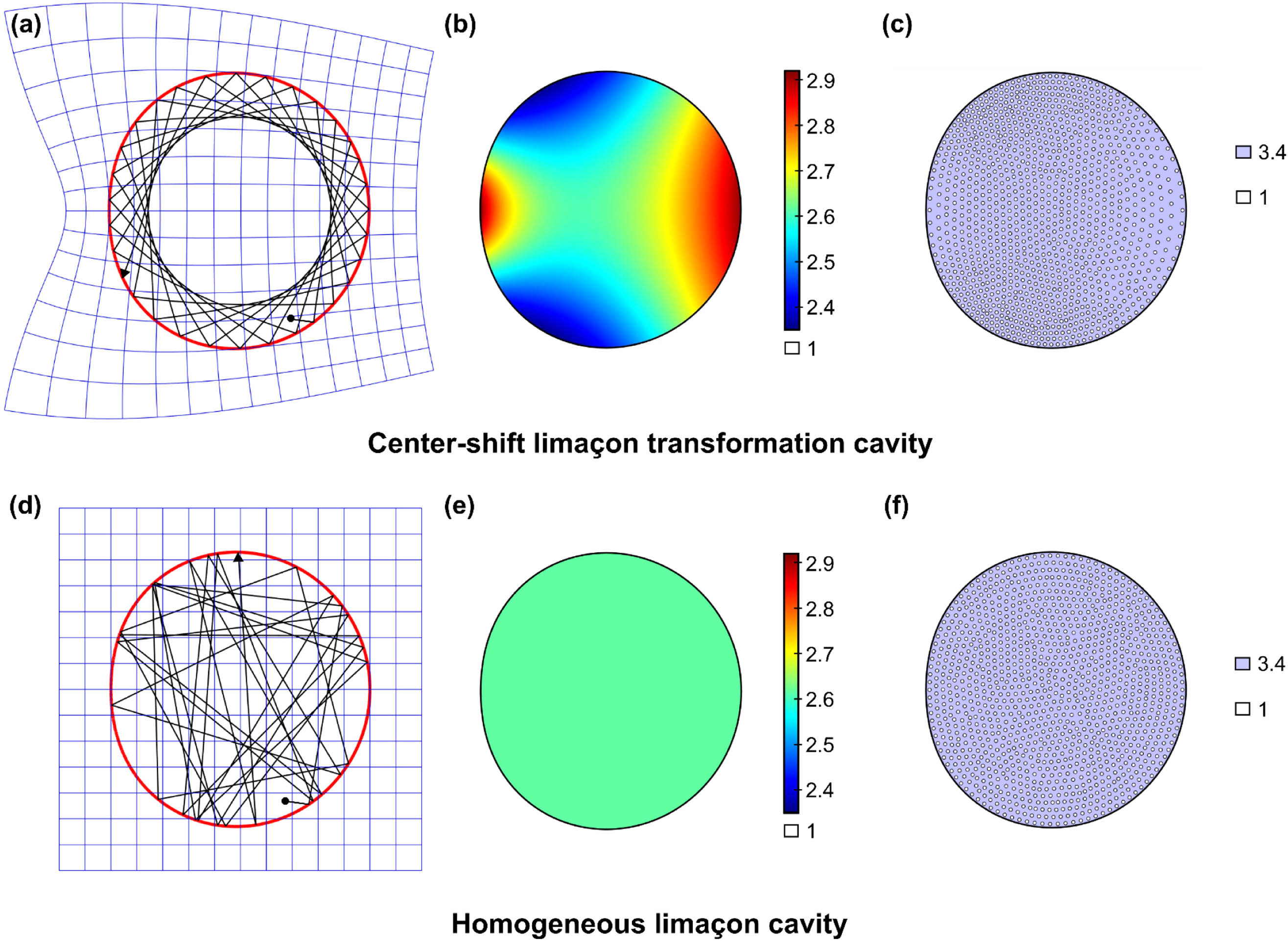
Figures 1(a) and 1(d) show ray trajectories in the CS limaçon TC and the corresponding homogeneous limaçon cavity, respectively. In the CS limaçon TC, the incident angles of the ray trajectory satisfying the TIR condition are preserved and the ray trajectory produces a caustic inside the TC. Figures 1(b) and 1(c) show a 2D continuous refractive index distribution and the corresponding 3D nanohole distribution for the realization of the CS limaçon TC, respectively. The high refractive index region has a low density of nanoholes, whereas the low refractive index region has a high density of nanoholes. In comparison with the CS limaçon TC, the ray trajectory of the homogeneous limaçon cavity [depicted in Fig. 1(d) and produced with the same initial condition as for Fig. 1(a)] shows a chaotic feature and illustrates that the incident angles of the ray do not always satisfy the TIR condition, resulting in refractive escape from the homogeneous cavity. Figures 1(e) and 1(f) show the counterpart homogeneous limaçon cavity with refractive index and a nanohole distribution for its implementation, respectively. The nanoholes of the homogeneous limaçon cavity are uniformly distributed such that its effective refractive index becomes 2.62. In addition to this, homogeneous disk cavity having the same area and the same mean refractive index as the CS limaçon TC was implemented similarly. Because the mean indices of the cavities are equal, the three cavities have nearly the same number of nanoholes, which guarantees almost the same amount of scattering loss due to the nanoholes for fair comparison of the three cavities. As our cavity lasers are fabricated with a TE-mode-oriented multi-quantum-well (MQW) wafer, we focused only on the TE resonant modes.
Figure 1.Ray trajectories, 2D refractive index profiles, and 3D nanohole distributions of a CS limaçon TC and the corresponding homogeneous limaçon cavity. (a) Well-ordered ray trajectory in the CS limaçon TC exhibiting similar caustic to a uniform disk. Curved blue lines are transformed images of the Cartesian grid lines in the original virtual space, and the red line is the boundary of a CS limaçon TC. (b) Two-dimensional CS limaçon TC and its refractive index profile. (c) Top view of 3D CS limaçon TC implemented by nanohole distribution. (d) Chaotic ray trajectory in the homogeneous limaçon cavity. The ray is launched with the same incident angle as in (a). Straight blue lines are grid of the Cartesian coordinates. (e) Homogeneous limaçon-shaped cavity having the same shape as the CS limaçon TC and its refractive index. (f) Top view of 3D homogeneous limaçon cavity implemented by the nanohole distribution.
Figure 2.Resonant mode patterns of the CS limaçon TC, the homogeneous limaçon cavity, and the homogeneous disk cavity. The free-space wavelengths of these resonant modes for all three cavities with 500 nm thickness are near 1550 nm (), which is the gain center of the InGaAsP-based WQM wafer. (a) Resonant mode (azimuthal mode number and radial mode number ) of the CS limaçon TC and its -factor . (b) Corresponding resonant mode of the homogeneous limaçon cavity and its -factor (). In contrast to the CS limaçon TC, the resonant mode pattern is distorted. (c) Resonant mode of the homogeneous disk cavity and its -factor ().
Figure 2 shows the TE resonant modes and their factors of the CS limaçon TC, the homogeneous limaçon cavity, and the homogeneous disk cavity (, , and , respectively) with the 3D nanohole structures, which are calculated by COMSOL Multiphysics 5.4a. Despite the deformed boundary of the CS limaçon TC, the factor of the TC mode is 4.2 times higher than that of the corresponding mode in the homogenous limaçon cavity and merely about 10% lower than that of the corresponding mode in the homogeneous disk cavity.
B. Fabrication of the Transformation Cavity Laser
For our demonstration, we epitaxially grew an InGaAsP-based MQW heterostructure on an InP(100) wafer using a metalorganic chemical vapor deposition (MOCVD) system. Subsequently, the spatially varying distribution of deep-sub-wavelength-scale nanoholes was fabricated on the epitaxially grown heterostructure wafer using electron-beam lithography and an inductively coupled plasma reactive ion etching (ICP-RIE) system. In the nanohole fabrication process, it is crucial that a hydrogen-dominant ICP-RIE condition should be used to minimize both the deterioration of the sidewall and the surface recombination effects [28].
Figures 3(a), 3(d), and 3(f) show scanning electron microscopy (SEM) images of the fabricated CS limaçon TC, homogeneous limaçon cavity, and homogeneous disk cavity, respectively. The diameter of the fabricated nanoholes is 60 nm and the distance between the centers of the nanoholes varies in the range of 100–240 nm to realize refractive index distribution inside the TC [Fig. 3(b)]. The reason for the absence of nanoholes near the center of the cavity is to secure the supporting post, which is necessary for a freestanding structure from the lateral etching process. This design alteration has very little effect on the high- resonant modes of interest because they are formed mainly along the boundary of the cavity. Through numerical simulations, we confirmed that the mode patterns and their factors were rarely affected by the design modification. The simulation results are included in Appendix A.3. Figure 3(h) shows a vertical cross-sectional SEM image of the fabricated nanoholes, and from this, one can note that high-aspect-ratio nanoholes are formed with high verticality by fully etching the 500 nm thick InGaAsP-based gain medium whose heterostructure is shown in Fig. 3(i). The steady-state room-temperature photoluminescence (PL) spectrum of our gain wafer is shown in Fig. 3(j), indicating that its gain center is located at 1580 nm. More details on the fabrication procedure can be found in the Appendix A.7.
Figure 3.(a) SEM image of the fabricated CS limaçon TC laser. (b) Top view image of the nanoholes structure. (c) Continuous 2D refractive index profile of the CS limaçon TC is overlapped to the mask design for visual aid. (d) and (f) SEM images of the fabricated homogeneous limaçon cavity and homogeneous disk cavity lasers. (e) and (g) Mask designs for the homogeneous limaçon cavity and homogeneous disk cavity, respectively; for visual aid, the green color represents the mean refractive index of the CS limaçon TC. (h) Vertical cross section of the nanohole structure. Protection carbon is deposited on the cavity to prevent structural collapse when vertical milling is carried out for visualization. (i) Vertical profile of the epitaxial heterostructure wafer. (j) Steady-state room-temperature photoluminescence spectrum of the epitaxial heterostructure wafer.
Figures 4(a) and 4(b) show a schematic of the experiment setup and the measured lasing characteristic curve of the CS limaçon TC laser, respectively. The lasing curve is obtained by tracing the first excited lasing mode because the most high- resonance among the resonances close to the gain center is expected to be excited. The relevant four-level lasing simulation result can be found in Appendix A. From the intersection point of the interpolated spontaneous emission line and the stimulated emission line, the lasing threshold can be estimated. One can see a clear transition from spontaneous emission to stimulated emission, which indicates the onset of the lasing. We measured lasing thresholds for eight samples of the CS limaçon TC laser for reproducibility, and their mean value is 88.3 μW. In Fig. 4(c), IR CCD images of the TC laser in action just before and after the threshold are shown. An abrupt change in brightness in the IR CCD images is observed across the lasing threshold, which implies the onset of stimulated emission. Figure 4(d) shows spectra at pumping powers of 92 μW and 108 μW. The FWHM lasing linewidth is 0.418 nm at 92 μW pumping power, and the linewidth becomes narrower to 0.215 nm at the increased pumping power of 108 μW. The inset of Fig. 4(d) shows the lasing spectrum at 123 μW pumping power in a wide range of wavelength, which exhibits single-mode lasing.
Figure 4.Measurement setup and lasing results for the three cavity lasers. (a) Schematic of experimental setup to measure lasing characteristics of the CS limaçon TC laser, the homogeneous limaçon cavity laser, and the homogeneous disk laser. OSA and BS mean optical spectrum analyzer and beam splitter, respectively. (b) Measured lasing curve of the CS limaçon TC laser. (c) CCD images of the TC laser in action just before and after the lasing threshold. (d) Lasing spectra of the CS limaçon TC laser at pumping power 92 μW and 108 μW. FWHMs at these pumping powers are 0.215 nm and 0.418 nm, respectively. An inset image depicts a spectrum at 123 μW pumping power, which shows single-mode lasing operation. (e) Lasing curves of the three cavity lasers for comparison. (f) The mean lasing thresholds and their standard deviations measured from every eight samples of the CS limaçon TC laser, the homogeneous disk cavity laser, and the homogeneous limaçon cavity laser are μ, μ, and μ, respectively.
To validate the restoration of degradation caused by the deformed boundary in our TC, we compared the lasing threshold of the CS limaçon TC with that of the corresponding homogeneous limaçon cavity and a disk cavity. Figure 4(e) shows the lasing curves of the CS limaçon TC, the homogeneous limaçon cavity, and the homogeneous disk cavity. The mean lasing thresholds of the three cavities are 88.3 μW, 256.6 μW, and 77.3 μW, respectively, which are depicted in Fig. 4(f). The mean lasing threshold of the CS limaçon TC is 65% less than that of the homogeneous limaçon cavity with the same shape but only 14% different from that of the homogeneous disk cavity. The lasing threshold is related with the factor of the excited single resonant mode near the threshold through the formula , where , , , and are the effective refractive index of the material, the resonance wavelength, the energy confinement factor, and the factor, respectively [29,30]. Ignoring the differences in , , and for the three microcavity lasers, the lasing threshold is inversely proportional to the factor. The calculated factors of the three cavities are qualitatively in accordance with the measured lasing thresholds.
3. CONCLUSION
In conclusion, we have demonstrated a CS limaçon TC laser, which was realized by deep sub-wavelength-scale nanoholes operating in an optical communication frequency regime with an InGaAsP-based MQW wafer. The presented CS limaçon TC exhibited a lasing threshold, a third of that of the corresponding homogeneous limaçon cavity, and moreover, the threshold of the CS limaçon TC was close to that of a homogeneous disk cavity, implying that spoiling caused by the boundary deformation was recovered by spatially varying nanohole density distribution designed by transformation optics and effective medium approximation. Because the boundary shape was a crucial factor in determining the evanescent coupling strength when a microcavity couples with another cavity or waveguide, this scheme can allow more flexibility in building whispering gallery microcavity devices. Our TC lasers were expected to contribute to cutting-edge light sources for integrated photonic circuits and highly sensitive chip-scale optical sensors, etc., through the modification of their geometrical shape as needed.
Acknowledgment
Acknowledgment. W.S.H. and H.K. were supported by ETRI grant funded by the Korea government (Development of Creative Technology for ICT).
APPENDIX A
Role of Möbius Mapping in Center-Shift Limaçon Mapping
In our TC design, we used a composite mapping of a conformal mapping and a subgroup of Möbius mapping ,
Figure 5 shows the refractive index distribution and grid when only the conformal mapping is used and when the conformal mapping is used after the subgroup of Möbius mapping . The subgroup of Möbius mapping reduces max-to-min refractive index of TC by shifting the center of the unit circle, and total mapping follows
By applying this mapping to the disk cavity with refractive index , the refractive index distribution of conformal TC can be obtained as follows:
In Eq. (A1), , which should be smaller than , is a size-shrinking factor to make the minimum refractive index higher than at the cavity boundary. is the maximum value that satisfies the following inequality, and when , the minimum refractive index at the boundary of the TC becomes the same as the refractive index before transformation,
From Fig. 5, one can note that the ratio of max-to-min refractive index and the maximum refractive index of CS limaçon TC are 1.24 and 2.92, respectively, when is 2.32. If Möbius mappings were not used, the ratio of the max-to-min refractive index and the maximum refractive index would be 2.55 and 4.5, respectively, which are too large for real implementation.
Figure 5.Effect of center-shift Möbius mapping on refractive index distribution. (a) A grid line and refractive index distribution of the unit disk with uniform index. (b) Using a conformal mapping to the unit disk. (c) Using the subgroup of Möbius mapping to the unit disk. (d) Using center-shift limaçon mapping to the unit disk.
Figure 6.Two-dimensional effective refractive index is obtained from a 60 nm diameter nanohole in a material with a refractive index of 3.4 and a thickness of 500 nm.
Figure 9.Various-shaped TCs and their implementation. (a) Refractive index distribution of a rounded-hexagon cavity. (b) Refractive index distribution of a stadium cavity. (c) Refractive index distribution of a rounded-isosceles triangle cavity. (d)–(f) Their design using a fixed size deep-sub-wavelength-scale hole for implementation.
The InGaAsP-MQW laser heterostructure was epitaxially grown on an on-axis -InP(100) wafer by an MOCVD system (D180 LDM, Veeco, Inc.). After growing a 400 nm thick etch-stop layer () on the InP wafer, 800 nm thick -InP was grown as a sacrificial layer for cavity floating. For the formation of a laser gain medium, a lattice-matched 220 nm thick layer for separate-confinement heterostructure (SCH), three-period (10 nm/6 nm) MQW, and 220 nm thick SCH layer were grown sequentially. The thickness of the InGaAsP-based layer for our cavities was approximately 500 nm. Additionally, a 0.6% compressive strain was applied to the MQW. In the growth process, the laser heterostructure was grown at 650°C under flow as an ambient carrier gas, and trimethylindium, trimethylaluminum, arsine, phosphine, and trimethylgallium were used as the precursors for the In, Al, As, P, and Ga sources, respectively.
Device Fabrication
After epitaxial growth, a 100 nm thick layer for a hard-etch mask was deposited on the as-grown laser heterostructure wafer by a plasma-enhanced chemical vapor deposition system (VL-LA-PECVD, Unaxis, Inc.), followed by a 200 nm thick positive-tone electron-beam resist (ZEP-520A, Zeon, Inc.). Subsequently, the etching region for the microcavity laser was defined using electron-beam lithography (JBX9300FS, Jeol, Inc.) at an acceleration voltage of 100 kV and beam current of 300 pA. To pattern the 60 nm diameter nanoholes and cavity boundaries, an exposure area dose of 340 and μ was used, respectively. Subsequently, the patterns were transferred to the layer using an ICP-RIE system (Versaline LL-ICP, Plasma Therm, Inc.) with a (45 sccm)/Ar (45 sccm) gas mixture. The ICP RF power was 500 W, bias power was 100 W, and working pressure was 3.5 mTorr. Using the patterned layer as a hard-etch mask, the 500 nm thick laser gain medium was dry etched by ICP-RIE with a hydrogen-dominant gas mixture () to minimize sidewall deterioration [28]. The gas flow rate of was 20/10/2 sccm, and the ICP/bias RF power was 800/125 W, respectively. To increase the volatility of the by-products and sidewall verticality, dry etching was conducted at a temperature of 200°C under a working pressure of 1.2 mTorr. Finally, the fabricated microcavity laser samples were dipped in a mixed solution of hydrochloric acid and phosphoric acid () to laterally etch the 800 nm thick -InP sacrificial layer, thereby leaving the freestanding cavity laser.
Laser Characterization
The top [Figs. 3(a), 3(b), 3(d), and 3(f)] and vertical cross-sectional [Figs. 3(h) and 3(i)] images of the fabricated limaçon microcavity lasers were obtained using field-emission SEM (SU8220, Hitachi, Inc.). The steady-state PL spectrum [Fig. 3(j)] of the as-grown MQW InGaAsP-based laser heterostructure was obtained using LabRAM HR-800 (Horiba Jobin Yvon Inc.) with a 514 nm line laser at room temperature. The fabricated microcavity lasers were optically pumped by a pulsed laser at a wavelength of 976 nm (BL976-SAG300, Thorlabs, Inc.) with a 2% duty cycle. The IR images of the operating microcavity lasers near the threshold [Fig. 4(c)] and their lasing characteristics [Figs. 4(b) and 4(d)–4(f)] were obtained using an IR-CCD [Widy SenS 640V-ST, New Imaging Technologies, Inc.] and an optical spectrum analyzer (MS9740B, Anritsu, Inc.), respectively.
References
[1] R. K. Chang, A. J. Campillo. Optical Processes in Microcavities, 3(1996).
Yong-Hoon Lee, Honghwi Park, Inbo Kim, Sang-Jun Park, Sunghwan Rim, Byoung Jun Park, Moohyuk Kim, Yushin Kim, Myung-Ki Kim, Won Seok Han, Hosung Kim, Hongsik Park, Muhan Choi, "Shape-tailored whispering gallery microcavity lasers designed by transformation optics," Photonics Res. 11, A35 (2023)