
Wang Jiangang, Gao Shiyou, Chen Xusheng, Zhang Mengyu. Mechanical Properties of A356 Aluminum Alloy after Laser Surface Remelting[J]. Chinese Journal of Lasers, 2020, 47(4): 402002
- Chinese Journal of Lasers
- Vol. 47, Issue 4, 402002 (2020)
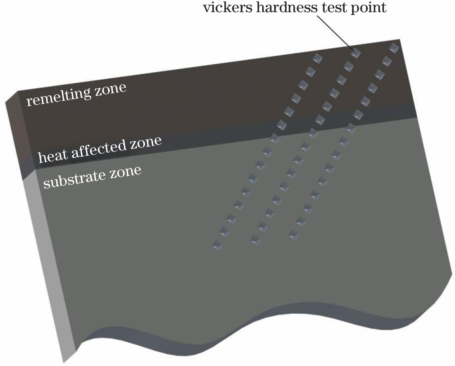
Fig. 1. Schematic of microhardness test points
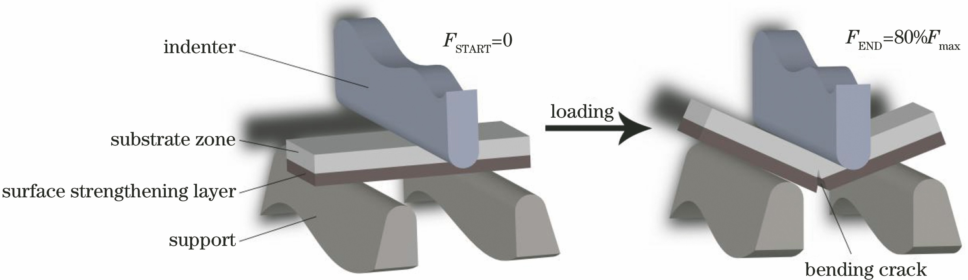
Fig. 2. Schematic of three-point bending experiment
Fig. 3. Microstructures of A356 aluminum alloy after laser remelting treatment at different power. (a) 1000 W; (b) 1500 W; (c) 2000 W
Fig. 4. Microstructures of remelting layer obtained at different laser power. (a) 1000 W; (b) 1500 W; (c) 2000 W
Fig. 5. EDS spectra of substrate area. (a) EDS test points distribution map; (b) EDS spectrum of Spot 1point; (c) EDS spectrum of Spot 2 point; (d) EDS spectrum of Spot 3 point
Fig. 6. XRD patterns of remelting layer obtained at laser power of 2000 W
Fig. 7. SEM images of each region in remelting layer obtained at laser power of 2000 W. (a) Remelting zone, ×1000; (b) heat affected zone, ×1000; (c) substrate zone, ×1000; (d) remelting zone, ×3000; (e) heat affected zone,×3000; (f) substrate zone, ×3000
Fig. 8. Microhardness diagrams. (a) Microhardness histogram; (b) microhardness of remelting layer obtained at laser power of 2000 W; (c) microhardness of remelting layer obtained at laser power of 1500 W; (d) microhardness of remelting layer obtained at laser power of 1000 W
Fig. 9. Bending test results. (a) Bending test results of substrate sample and remelting samples obtained at different laser power; (b) partial view of Fcr for A356 base metal; (c) partial view of Fcr for remelting sample obtained at laser power of 1000 W; (c) partial view of Fcr for remelting sample obtained at laser power of 1500 W; (d) partial view of Fcr for remelting sample obtained at laser power of 2000 W
Fig. 10. Metallographic images of bending cracks in different samples. (a) A356 aluminum alloy base material; (b) remelting sample obtained at laser power of 1000 W; (c) remelting sample obtained at laser power of 1500 W; (d) remelting sample obtained at laser power of 2000 W
|
Table 1. Chemical composition of A356 aluminum alloy
|
Table 2. ESD results of substrate area
| ||||||||||||||||||||||||
Table 3. Size of each phase in remelting layer obtained at different laser power

Set citation alerts for the article
Please enter your email address
© Copyright 2018-2021 | Chinese Laser Press. All Rights Reserved 沪ICP备15018463号-20