
Lidong Yu, Tianxuan Bian, Yunteng Qu, Beibei Zhang, Yang Bai. Effect of Laser Parameters on Corrosion Resistance of Laser Melting Layer on Q235B Steel Surface[J]. Chinese Journal of Lasers, 2023, 50(8): 0802201
- Chinese Journal of Lasers
- Vol. 50, Issue 8, 0802201 (2023)
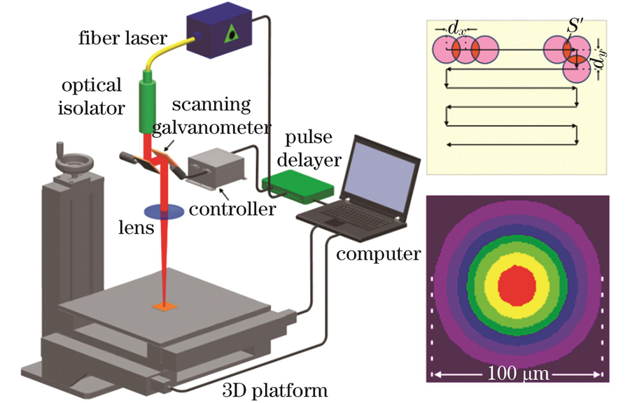
Fig. 1. Schematic of laser melting unit, where the inset shows laser beam scanning path and two-dimensional energy distribution
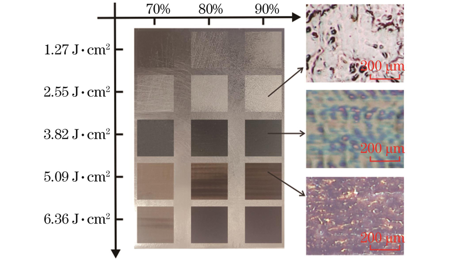
Fig. 2. Macroscopic and microscopic images of laser melting layer
Fig. 3. Dynamic potential polarization curves of laser melting layer at different laser single pulse energy densities and spot overlap rates
Fig. 4. SEM images of laser melting layers with optimal laser single pulse energy density and different spot overlap rates for a single laser scanning. (a) β=70%; (b) β=80%; (c) β=90%
Fig. 5. Dynamic potential polarization curves of laser melting layer with different laser scanning times (Eopt=3.82 J/cm2 and β=80%)
Fig. 6. SEM images of laser melting layers with different laser scanning times n (Eopt=3.82 J/cm2 and β=80%). (a) n=1; (b) n=2;
Fig. 7. Sectional SEM image of optimal laser melting layer
Fig. 8. EDS spectra and XRD patterns of tested samples. (a) EDS spectrum of substrate; (b) EDS spectrum of alkaline blackening layer; (c) EDS spectrum of optimal laser melting layer; (d) XRD patterns
Fig. 9. Electrochemical test of corrosion resistant layers. (a) Dynamic potential polarization curves; (b) Nyquist curves; (c) Bode plots
Fig. 10. EIS equivalent circuit
Fig. 11. Microscopic morphologies of two corrosion resistant layers. (a)(d) Thickness of cut surfaces; (b)(e) three-dimensional
|
Table 1. Single pulse energy density at different average laser powers
|
Table 2. Parameters related to kinetic potential polarization curves at different laser single pulse energy densities and spot overlap rates in a single laser scanning
|
Table 3. Parameters related to kinetic potential polarization curves with different laser scanning times (Eopt=3.82 J/cm2 and β=80%)
| ||||||||||||||||||||||||||||||||||||||||||||||||||||||||||||
Table 4. EDS analysis data at different thicknesses on the section of optimal laser melting layer
| |||||||||||||||||||
Table 5. EDS analysis data of samples to be tested
|
Table 6. Fitting parameter values of EIS equivalent circuit


Set citation alerts for the article
Please enter your email address

© Copyright 2018-2021 | Chinese Laser Press. All Rights Reserved 沪ICP备15018463号-20