• Acta Photonica Sinica
  • Vol. 49, Issue 10, 1031002 (2020)
Jian WANG, Jun-qi XU, Jun-hong SU, Yang LI, and Yun-yun SHI
Author Affiliations
  • Shaanxi Province Thin Film Technology and Optical Test Open Key Laboratory,Xi'an Technological University,Xi'an 710021,China
  • show less
    DOI: 10.3788/gzxb20204910.1031002 Cite this Article
    Jian WANG, Jun-qi XU, Jun-hong SU, Yang LI, Yun-yun SHI. Research on Infrared Anti-reflection Thin Film Devices with Compatibility of Electromagnetic Shielding[J]. Acta Photonica Sinica, 2020, 49(10): 1031002 Copy Citation Text show less
    Microstructure of grid under 100× optical microscopy
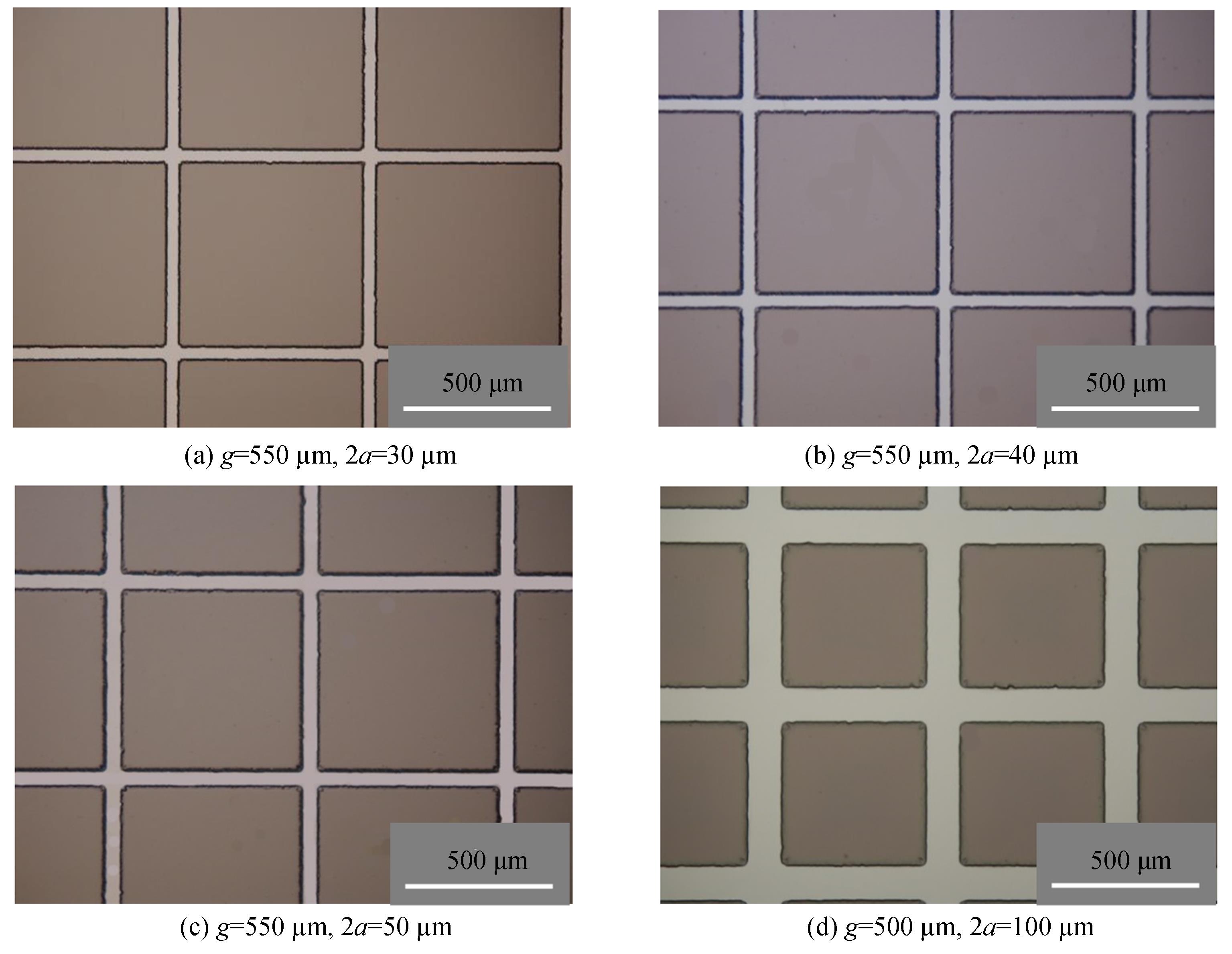
    Fig. 1. Microstructure of grid under 100× optical microscopy
    Microstructure of metal grid film
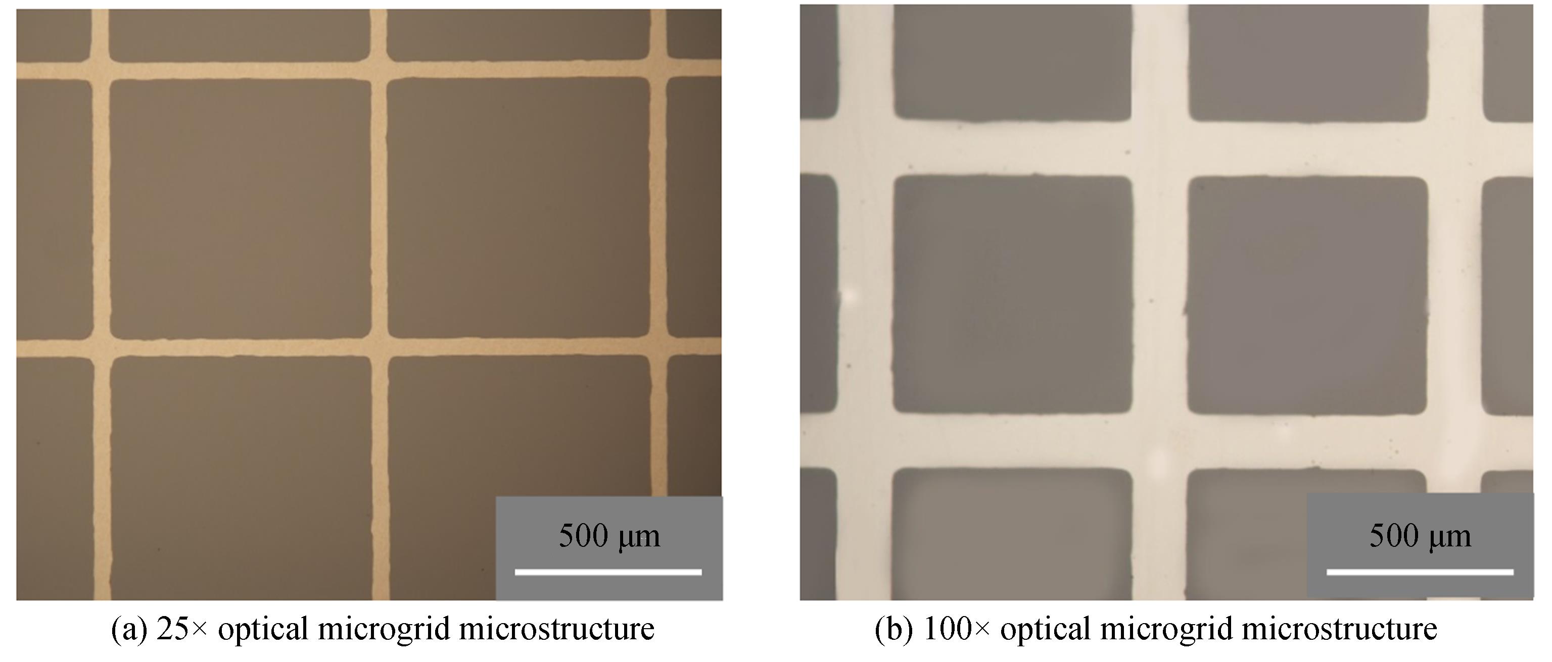
    Fig. 2. Microstructure of metal grid film
    Matrix method for solving multilayer films
    Fig. 3. Matrix method for solving multilayer films
    Simulation curve of infrared antireflection coating in 3~5 μm band
    Fig. 4. Simulation curve of infrared antireflection coating in 3~5 μm band
    Transmittance-shielding efficiency test curve of metal grid
    Fig. 5. Transmittance-shielding efficiency test curve of metal grid
    The measured curve of infrared antireflection coating in the 3~5 µm band
    Fig. 6. The measured curve of infrared antireflection coating in the 3~5 µm band
    Structure diagram of thin film device compatible with electromagnetic shielding infrared window
    Fig. 7. Structure diagram of thin film device compatible with electromagnetic shielding infrared window
    Transmittance-electromagnetic shielding effectiveness of thin film device
    Fig. 8. Transmittance-electromagnetic shielding effectiveness of thin film device
    CraftsmanshipTime/sTemperature /℃
    Ultrasonic cleaning600(10 min)60
    Spin-on photoresist12(low speed 800 r/min)25
    20(high speed 2 000 r/min)25
    Bake9090
    Exposure1525
    Development1525
    Table 1. Photolithography process parameters of the grid
    Film materialTemperature/℃Evaporation methodBeams/mA

    Vacuum degree of

    work/(×10-2 Pa)

    Deposition rate/

    (nm·s-1)

    Cu120Electron beam evaporation heat1001.00.53
    Cr300.34
    Table 2. Shows the metal film preparation process
    Film materialTemperature/℃Evaporation methodBeams/mA

    Vacuum degree of

    work/(×10-2Pa)

    Deposition rate/

    (nm·s-1)

    ZnSe170Electron beam evaporation heat301.00.23
    BaF20.97
    Table 3. Thin film preparation process parameters
    Line width 2a/µm20304050
    Average transmittance before antireflection coating/%50.348.546.145.0
    Average transmittance after antireflection coating/%91.886.184.380.6
    Increment Δ/%40.537.638.235.6
    Table 4. Comparison of transmittance before and after the infrared antireflective coating on the metal grid

    SE/dB

    2a/μm

    M20M30M40M50S20S30S40S50
    Si substrate4.24.24.24.223.023.023.023.0
    Film16.617.019.420.527.929.029.833.1
    Metal mesh12.412.815.216.34.96.06.810.1
    Table 5. Electromagnetic shielding effectiveness of electromagnetic shielding infrared window film devices
    Jian WANG, Jun-qi XU, Jun-hong SU, Yang LI, Yun-yun SHI. Research on Infrared Anti-reflection Thin Film Devices with Compatibility of Electromagnetic Shielding[J]. Acta Photonica Sinica, 2020, 49(10): 1031002
    Download Citation