The State Key Laboratory of High Performance Complex Manufacturing, College of Mechanical and Electrical Engineering, Central South University, Changsha 410083, China
A fused silica glass micro-channel can be formed by chemical etching after femtosecond laser irradiation, and the successful etching probability is only 48%. In order to improve the micro-channel fabrication success probability, the method of processing a high-temperature lattice by a femtosecond laser pulse train is provided. With the same pulse energy and scanning speed, the success probability can be increased to 98% by optimizing pulse delay. The enhancement is mainly caused by the nanostructure, which changes from a periodic slabs structure to some intensive and loose pore structures. In this Letter, the optimum pulse energy distribution ratio to the etching is also investigated.
A femtosecond laser with extremely high peak power and ultra-short pulse duration is widely applied in fabricating a waveguide[1], a grating[2–5], a microfluidic channel[6], and other functional devices[7–9] in fiber[10,11], fused silica glasses[12,13], [14], and other transparent materials. Since the micro-channel fabricated by a femtosecond laser in combination with chemical etching[15] can have a high depth to diameter ratio, it has many potential applications in biological and chemical analysis. However, because of some texture defects in the material, the uniformity of the micro-channel is too low to be carried in practical fabrication. Although some researchers have tried to use the KOH solution or a special photostructurable glass, and the etching rate can be improved, the successful etching rate is slightly changed. Therefore, it is imperative to find a solution for improving the probability of successful etching.
After the first laser pulse ablation, the electrons are motivated from the valence band to the conduction band by multi-photon absorption and other ionization, which will sustain a few hundred per second[16,17]. Subsequently, the effect of electron–electron collisional ionization occurs, and the electron energy is transferred to the lattice. When the lattice temperature is over the relevant threshold[18], the permanent material modification can occur. The lattice becomes coupled with these free electrons during a period of less than a picosecond to several tens of picoseconds, depending upon the material[19,20]. The thermal energy absorbed by the lattice needs a few microseconds to dissipate. When the second pulse arrives, the femtosecond laser processing high-temperature lattice can be formed. Although some research has reported that the femtosecond pulse train can improve the etching rate, this is mainly based on the metallic transition of melted silicon with the corresponding absorption efficiency, or the electron excitation by the first pulse[21], which is different from the method described in this Letter.
The relationship between the etching rate and scanning speed, pulse delay, pulse energy, and distribution ratio has been studied in Ref. [15]. However, in their experiment, the time delay is very small. In this Letter, we show that a time delay of 300 ps can be achieved, which obtains more interesting results. The relationship between the time delay and the peak of the modification region is observed. Except in special circumstances, each parameter scans five times per experiment. In each of the scanning processes, the energy of the pulse and the scanning speeds are always kept as a constant. After being irradiated, the sample is refreshed by the ultrasonic wave, and then etched in aqueous solution of HF acid at room temperature.
Sign up for Chinese Optics Letters TOC. Get the latest issue of Chinese Optics Letters delivered right to you!Sign up now
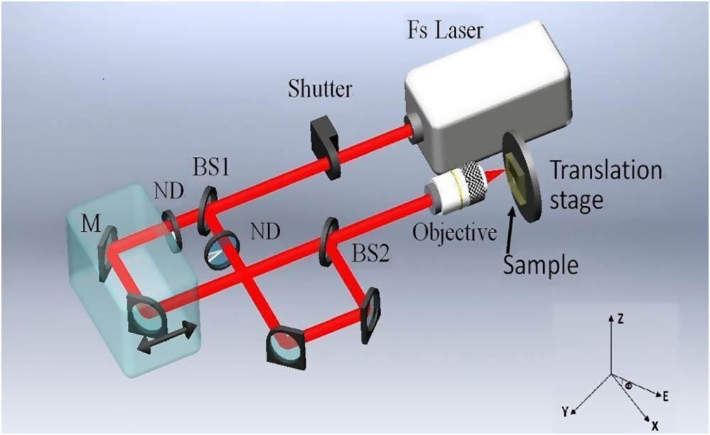
The schematic diagram shows the setup of the experiment of the ultrafast double pulse femtosecond lasers’ fabrication system (Fig. 1). The laser source (Spectra-Physics, Inc.) has a central wavelength of 800 nm, pulse width of 120 fs, and repetition of 1 kHz. The beam is first split by a 5/5 beam splitter (BS1), and then spatially overlapped using BS2. The beam is focused into the samples by a 10 times objective lens with a numerical aperture (NA) of . The glass samples of 1.0 mm thick are mounted on a computer-controlled three-axis translation stage, as shown in Fig. 1. The energies of the two pulses can be individually adjusted by the neutral density attenuator. After irradiation, the sample was cut into two sections along the YZ plane. One half was polished from the entrance of the micro-channel (YZ plane) and immersed in a 5% HF solution at room temperature (20°C) to produce a micro-channel. The other half of the silica glass was cut and polished parallel to the XZ plane to observe the laser-modified zones by a scanning electron microscope (SEM).
Figure 1.Schematic diagram of the ultrafast double pulse femtosecond lasers fabrication system. M, mirror; ND, neutral density attenuator.
First, the experiment with different time delays and polarization is conducted. Taking into account the influence of the polarization state, the results show that when the angle between the electric vector and the scanning direction (write for ) is 0°, the solution is virtually obstructed by the modified thin slabs, which is similar to Ref. [22]. Thus, the time delay between the double pulses has little effect on the success probability. When the is 90°, the periodic nanostructures formed in the fused silica glasses are oriented perpendicular to the polarization, and the success probability of corrosion has a lot to do with the time delay.
The micro-structure of the processing grooves is analyzed from the other half of the sample. It is found that when is 0°, the processing morphology appears as a half-spherical tank structure, while when the is 90°, it appears as a rectangular groove structure that may have different functions in the device, as shown in Figs. 2(a) and 2(b).
Figure 2.Top view (XZ plane) SEM images (a) where is 0°; (b) where is 90°.
To explore the probability of success of corrosion enhancement due to the different time delay ablation method, we conducted a series of experiments. We use a range of time delays from 100 fs to 300 ps. The single pulse scanning speed is 0.2 mm/s, and the total energy is 3 mW; this remains the same with the double pulse. Based on a large number of experiments, we found that for the conventional single pulse after femtosecond laser processing and chemical etching the probability of success of corrosion is approximately 48% or less. When the time delay was increased to 1 ps, the probability of success of corrosion increased significantly, reaching about 98%. Figure 3(b) shows the relationship between the etching rate and delay time. It was evident that the etching rate was increased with the time delay, and when the time delay was increased to 300 ps, the etching rate was almost equal to a single pulse. It was also found that due to the nonuniform processing and the defects of the material itself, the micro-channel could not be etched after femtosecond laser irradiation, as shown in Fig. 3(a), where some of the micro-channels were not etched when , and 200 fs is that case. While as the time delay increased, the inconsistency of processing is overcome by the advantages of the double pulse processing. Compared with , when the etching result becomes more uniform.
Figure 3.(a) Microscopic images of the etched micro-channel irradiated by different time delays. (b) Etching rate of a single pulse and a double pulse.
Previous research has found that the ablation is strongest when the two laser pulses overlap[23]. When the separation between the two pulses is increased, the second pulse is largely blocked, which will cause less ablation, and the time frame is less than 1 ps due to the plasma. When the time delay is further increased to longer than a few picoseconds, the plasma formed by the first pulse will scattered, and the reflection of the second pulse will be decreased. The thermal energy from the first pulse irradiation has not dissipated; the second pulse contributes to reproducing the high-temperature lattice. They also found that there was spontaneous formation of a periodical array composed of nano-sized spherical voids in commercial borosilicate glass under femtosecond laser irradiation at a low repetition rate of 1 kHz[24]. The size and the shape of the modification region will be related to the double pulse parameters.
In our experiment, since the etching solution was uniform, the explanation for previous results should be the difference of micro-structures caused by different laser processing. Figure 4 shows the SEM images of the periodic nanostructures formed by a femtosecond laser irradiated in combination with chemical etching. At a low time delay of , the nanostructures are regular slabs. At the time delay threshold of , the probability of success of corrosion is significantly enhanced, and while the etching rate is slow, the laser-induced modification contains slabs and porous sections. When the time delay is greater than 100 ps, the laser-irradiated zones are mainly porous.
Figure 4.Side view (YZ plane) the light entrance SEM images of long range periodic nanostructures formed by different time delays after being polished and shortly etched. (a) ; (b) ; (c) .
According to the experiment results, for double pulse irradiation, when the time delay is more than 1 ps, the electrons excited by the first pulse will degenerate[25]. The energy absorption efficiency is still at a higher level. The thermal diffusion time of the fused silica glass is longer than the time delay, which is approximately a few microseconds. When the time delay overlaps the relaxation time of conduction band electrons, the energy will be transferred to the crystal lattice by the electrons. Then, the conduction band electrons almost relax to the defect state and may recombine with the holes with phonon emission. But, the former pulse, which is crucial to the whole manufacturing process, will act as a pre-conditioner, and the resulting pulse will reheat the material and induce the permanent material modification[26]. Experiments show that a femtosecond laser processing high-temperature lattice would make the irradiated zones become loose porous structures.
In the capillary, the height of the liquid can be written as
Parameter is the radius of the pore. So, the rising height of the liquid is inversely proportional to the radius. Therefore, as the time delay increases further, the HF solution enters more easily.
We also studied the optimum pulse energy distribution ratio to understand which of the pulses was more important for the corrosion and optimizing manufacturing parameters when the time delay was great enough. The time delay also ranges from 0 to 300 ps, and the energy distributions are , , and , respectively. Each data point represents an average of five experiment’s data, and the error bars are shown in Fig. 5. When is smaller than 100 fs, we should use low energy instead of high for fabrication, because during this time the electrons are motivated from the valence band to the conduction band. The greater energy of the second pulse will stimulate the electrons to a high energy band, resulting in other features. When the is roughly equivalent to 100 fs, the etching rate is severely suppressed regardless of the pulse energy distribution ratio. When is in the range of 100 fs to 100 ps, and the energy of the second pulse is less than or equal to the energy of the first pulse, the plasma caused by the first pulse will easily block the effect of the second pulse. This leads to difficulties with corrosion, while the larger second pulse can more easily affect the medium. At the energy distribution ratio of , the plasma may reflect the second pulse more markedly. After becomes 100 ps, the plasma completely disappears. The etching effect depends on the quantity of the high-temperature lattices produced by the first pulse. So, and will show the same etching rate. Compared with , the superior high-temperature lattices will absorb less energy equally, so the energy distribution ratio of has a poor etching rate.
Figure 5.Relationship between the etching depth and the pulse energy ratio.
In conclusion, this method of femtosecond laser processing high-temperature lattice, can improve etching rates and the probability of successful corrosion when compared to traditional femtosecond laser processing. The greater probability of successful corrosion is mainly due to the periodic nanostructure’s change from line slabs to becoming porous. Because the rising height of the liquid is inversely proportional to the radius in the capillary, the porous nanostructure improves the ability for the solution to enter the modified area. The experiments also demonstrate that when the pulse delay is smaller than 100 ps or larger than 100 ps, the energy distribution ratio of is better for etching. When due to the plasma caused by the first pulse, which blocks the effect of the second pulse, the greater energy of the second pulse will cause a high etching rate.