
Shuirou WANG, Heming CHEN, Xue LIU, Wanle PAN. An Integrated Device for Electro-optic Modulation and Wavelength Division Multiplexing with the Wavelength Channel Spacing of 3.2 nm[J]. Acta Photonica Sinica, 2022, 51(5): 0551312
- Acta Photonica Sinica
- Vol. 51, Issue 5, 0551312 (2022)
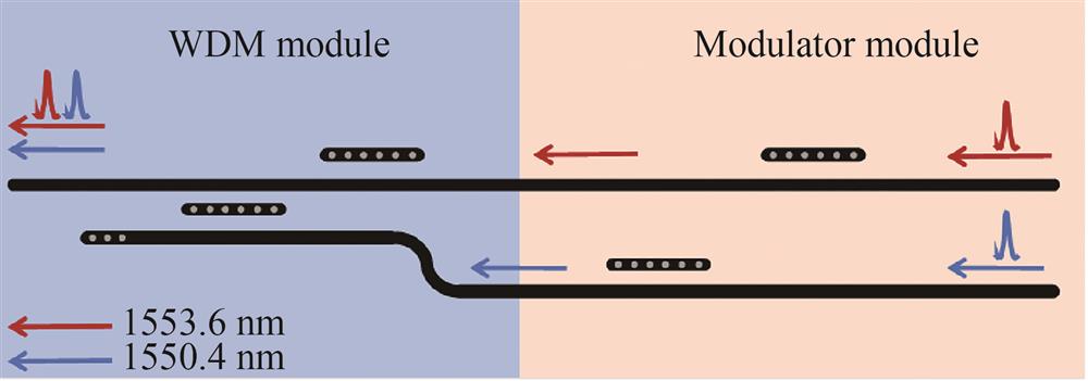
Fig. 1. Working principle of integrated device based on photonic crystal electro-optic modulation and wavelength division multiplexing
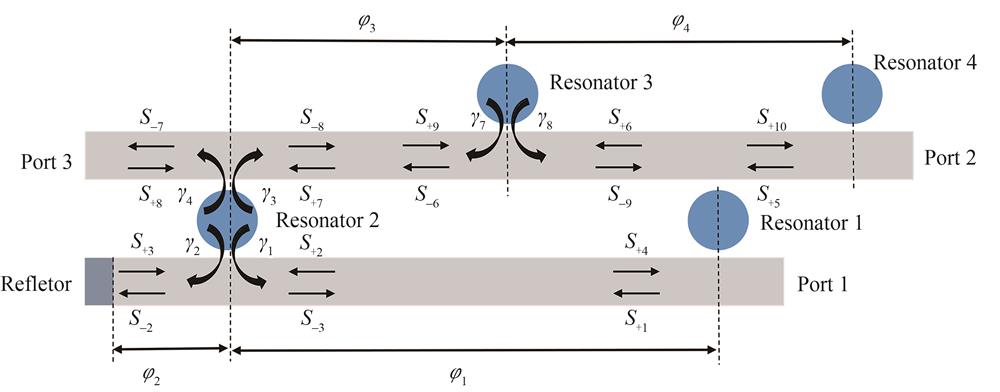
Fig. 2. Theoretical model of integrated device based on photonic crystal electro-optic modulation and wavelength division multiplexing
Fig. 3. Three-dimensional structure of integrated devices based on electro-optic modulation and wavelength division multiplexing
Fig. 4. Structural diagram of one-dimensional photonic crystal nanobeam cavity
Fig. 5. Structural diagram of side-coupling between one-dimensional photonic crystal nanobeam cavity and nanowire waveguide
Fig. 6. The influence of Nr on transmittance and resonance wavelength
Fig. 7. The influence of
Fig. 8. Electro-optic modulator structure diagram
Fig. 9. Schematic diagram of electro-optic modulator doping structure
Fig. 10. Carrier density distribution diagram when the voltage across both ends is 1.25 V
Fig. 11. Modulation reflectance spectra "on" and "off" states
Fig. 12. Structure diagram of wavelength division multiplexing module
Fig. 13. Transmission spectrum of each port of wavelength division multiplexing module
Fig. 14. Steady-state field distribution diagram of wavelength division multiplexing
Fig. 15. Overall integrated device structure diagram
Fig. 16. Steady-state field distribution diagram of integrated devices
Fig. 17. Transmission spectrum of integrated device when the modulation state is "on" and "off"
Fig. 18. Simulation calculation of the stable time in the "on" and "off" states
Fig. 19. The influence of variation of center holes radius on insertion loss
| |||||||||||||||||||||||
Table 1. Performance parameters of integrated devices
|
Table 2. Comparison with state-of-the-art integrated device for electro-optic modulation and wavelength-division multiplexing

Set citation alerts for the article
Please enter your email address
© Copyright 2018-2021 | Chinese Laser Press. All Rights Reserved 沪ICP备15018463号-20