• Chinese Physics B
  • Vol. 29, Issue 9, (2020)
Xiao-Ping Ma1, Hong-Guang Piao1、†, Lei Yang1, Dong-Hyun Kim2, Chun-Yeol You3, and Liqing Pan1
Author Affiliations
  • 1Research Institute for Magnetoelectric & Weak Magnetic-field Detection, College of Science, China Three Gorges University, Yichang 443002, China
  • 2Department of Physics, Chungbuk National University, Cheongju 8644, Chungbuk, Republic of Korea
  • 3Department of Emerging Materials Science, Daegu Gyeongbuk Institute of Science and Technology (DGIST), Daegu 42988, Republic of Korea
  • show less
    DOI: 10.1088/1674-1056/aba09a Cite this Article
    Xiao-Ping Ma, Hong-Guang Piao, Lei Yang, Dong-Hyun Kim, Chun-Yeol You, Liqing Pan. Asymmetric dynamic behaviors of magnetic domain wall in trapezoid-cross-section nanostrip[J]. Chinese Physics B, 2020, 29(9): Copy Citation Text show less
    (a) The geometry and dimension of the trapezoid-cross-section nanostrip. The external magnetic field direction is denoted by the arrows on the top. A head-to-head transverse DW is initially positioned in the center of the nanostrip, and its direction is denoted by the arrows inside. The cross section of the nanostrip is shown at the bottom. (b) The schematic diagrams of the nanotube unrolled into a trapezoid-cross-section nanostrip when it is cut along the long axis.
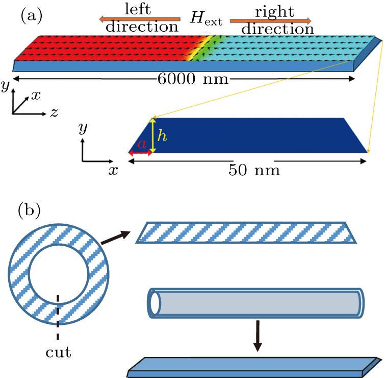
    Fig. 1. (a) The geometry and dimension of the trapezoid-cross-section nanostrip. The external magnetic field direction is denoted by the arrows on the top. A head-to-head transverse DW is initially positioned in the center of the nanostrip, and its direction is denoted by the arrows inside. The cross section of the nanostrip is shown at the bottom. (b) The schematic diagrams of the nanotube unrolled into a trapezoid-cross-section nanostrip when it is cut along the long axis.
    The absolute value of DW displacement varies with time driven by (a) ±10 Oe, (b) ± 35 Oe and (c) ± 50 Oe magnetic field in the case of a = 10, h = 5 nm. In (a), the red and black curves coincide. The symbols ↑, ↓, and ⊙, ⊗ represent the spin structure of transverse and anti-vortex DWs in xz-plane (top view), and the corresponding images is illustrated beside the symbols. The arrows inside the images as well as the color map represent the in-plane magnetization directions. The white/black dot in the images indicates an upward/downward anti-vortex core.
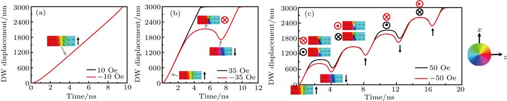
    Fig. 2. The absolute value of DW displacement varies with time driven by (a) ±10 Oe, (b) ± 35 Oe and (c) ± 50 Oe magnetic field in the case of a = 10, h = 5 nm. In (a), the red and black curves coincide. The symbols ↑, ↓, and ⊙, ⊗ represent the spin structure of transverse and anti-vortex DWs in xz-plane (top view), and the corresponding images is illustrated beside the symbols. The arrows inside the images as well as the color map represent the in-plane magnetization directions. The white/black dot in the images indicates an upward/downward anti-vortex core.
    The schematic diagrams of the directions of the local magnetization M. The magnetic torque τ on M and the demagnetizing field Hd (cross section view) is shown on the left panel of (a). The snapshots of the y-component demagnetizing field (Hd,y) distribution around the DW (cross section view) at t = 5 ns driving by ± 10 Oe fields are illustrated on the right panel of (a). The color bar indicates the Hd,y value. The nanostrip is artificially divided into 5 layers as shown in the inset of (c). The Hd,y for different layers is shown in (b) driven by +10 Oe field and (c) –10 Oe field in the case of a = 10 nm and h = 5 nm.
    Fig. 3. The schematic diagrams of the directions of the local magnetization M. The magnetic torque τ on M and the demagnetizing field Hd (cross section view) is shown on the left panel of (a). The snapshots of the y-component demagnetizing field (Hd,y) distribution around the DW (cross section view) at t = 5 ns driving by ± 10 Oe fields are illustrated on the right panel of (a). The color bar indicates the Hd,y value. The nanostrip is artificially divided into 5 layers as shown in the inset of (c). The Hd,y for different layers is shown in (b) driven by +10 Oe field and (c) –10 Oe field in the case of a = 10 nm and h = 5 nm.
    (a) The Edemag and Eex profiles versus time driven by 50 Oe magnetic field. (b) The sum of Edemag and Eex versus time. The snapshots of anti-vortex walls and transverse walls in xz-plane (top view) are shown on the top and bottom of (b), respectively. The arrows inside the snapshots as well as the color map represent the in-plane magnetization directions.
    Fig. 4. (a) The Edemag and Eex profiles versus time driven by 50 Oe magnetic field. (b) The sum of Edemag and Eex versus time. The snapshots of anti-vortex walls and transverse walls in xz-plane (top view) are shown on the top and bottom of (b), respectively. The arrows inside the snapshots as well as the color map represent the in-plane magnetization directions.
    The DW average velocity v under different magnetic fields in the cases of (a) a = h = 5 nm, (b) a = h = 8 nm and (c) a = 10 nm, h = 5 nm.
    Fig. 5. The DW average velocity v under different magnetic fields in the cases of (a) a = h = 5 nm, (b) a = h = 8 nm and (c) a = 10 nm, h = 5 nm.
    Xiao-Ping Ma, Hong-Guang Piao, Lei Yang, Dong-Hyun Kim, Chun-Yeol You, Liqing Pan. Asymmetric dynamic behaviors of magnetic domain wall in trapezoid-cross-section nanostrip[J]. Chinese Physics B, 2020, 29(9):
    Download Citation