
Han Wu, Jing-Yu Wu, Zhuo Chen. Strong coupling between metasurface based Tamm plasmon microcavity and exciton [J]. Acta Physica Sinica, 2020, 69(1): 010201-1
- Acta Physica Sinica
- Vol. 69, Issue 1, 010201-1 (2020)
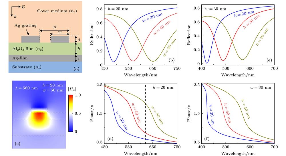
Fig. 1. (a) A schematic diagram of metasurface consisting of silver grating, alumina dielectric layer and silver film, in which the thickness of silver film, the period and thickness of silver grating are fixed at t = 30 nm, P = 150 nm and d = 10 nm, respectively; (b), (d) the thickness of alumina layer is h = 20 nm, and the reflection spectrum and phase of metasurface at different width of silver grating; (c) the magnetic field distribution of metasurface at resonance with grating width w = 50 nm and alumina layer thickness h = 20 nm; (e), (f) with grating width w = 30 nm and different thickness of alumina layer have reflected spectra and phases on the metasurface.
(a)银光栅-氧化铝介质层-银薄膜构成的超表面结构示意图, 其中银薄膜厚度、银光栅周期和厚度分别固定为t = 30 nm, p = 150 nm和d = 10 nm; (b), (d)氧化铝层厚度h = 20 nm银光栅同宽度时超表面的反射谱和反射位相; (c)光栅宽度w = 50 nm和氧化铝层厚度h = 20 nm的超表面在共振时的磁场分布图; (e), (f)银光栅宽度w = 30 nm氧化铝层厚度不同时超表面的反射谱和反射位相
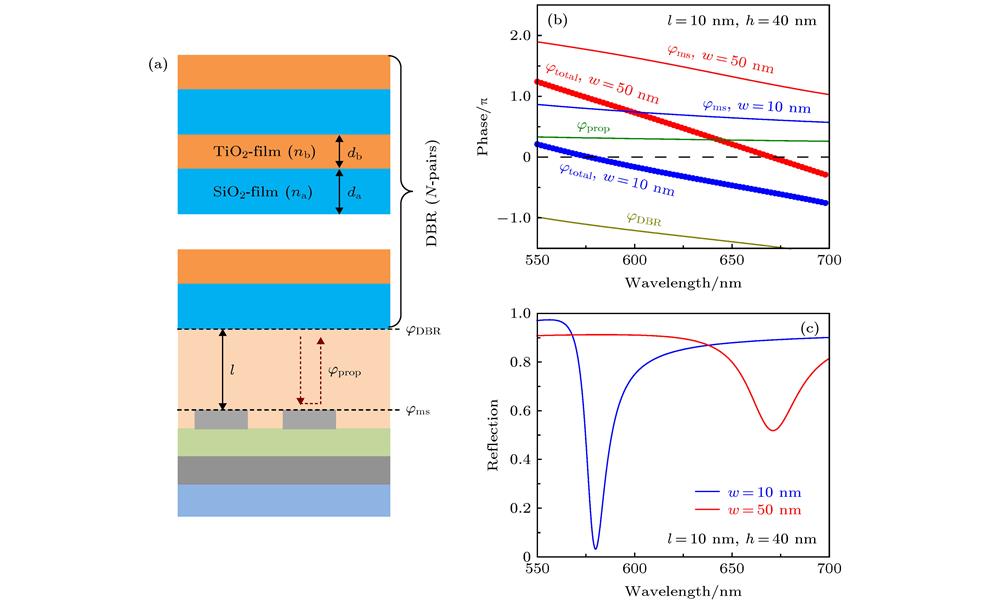
Fig. 2. (a) A schematic diagram of the structure of a Tamm plasmon microcavity consisting of metasurface-dielectric spacer-DBR. DBR consists of 8 pairs of silica and titanium dioxide multilayer dielectric films, in which the refractive index of silica is n a = 1.45, the refractive index of titanium dioxide is n b = 2.4, and the thickness of silica and titanium dioxide in each layer is d a = 103.5 nm and d b = 62.5 nm. The thickness of the dielectric spacer is l , and the refractive index is the same as that of the cladding layer of the metasurface structure in Fig. 1(a) . The structural parameters of the metasurface are the same as those shown in Fig. 1(a) . The phase transitions of φ DBR and φ metal are caused by the reflection of light on the surface of DBR and metasurface structure respectively. φ prop represents the phase of light propagating in the dielectric spacer; (b) the thickness of fixed dielectric spacer is l = 10 nm, the thickness of alumina layer in metasurface is h = 40 nm, and the width of silver grating is w = 10 nm and 50 nm. In both cases, the relationship between wavelength and the obtained φ ms, φ DBR, φ prop and total phase φ total is obtained. The horizontal dashed line represents the phase of 0; (c) reflectance spectra of metasurface-dielectric spacer-DBR structures at l = 10 nm, h = 40 nm and w = 10 nm and 50 nm.
(a)由超表面-介质间隔层-DBR构成的Tamm等离激元微腔结构示意图. DBR由8对二氧化硅和二氧化钛多层介质膜组成, 其中二氧化硅和二氧化钛的折射率为n a = 1.45和n b = 2.4, 厚度为d a = 103.5 nm和d b = 62.5 nm; 介质间隔层厚度为l , 折射率与图1(a) 中超表面结构的包覆层折射率相同, 超表面的结构参数与图1(a) 中所展示的相同. φ DBR和φ metal分别是光在DBR的表面和超表面结构的表面反射引起的位相变化, φ prop代表光在介质间隔层中的传播位相; (b)固定介质间隔层厚度为l = 10 nm, 超表面中氧化铝层厚度为h = 40 nm, 银光栅宽度为w = 10 nm和50 nm两种情况下所获得的φ ms以及φ DBR, φ prop, 总位相φ total随波长的变化关系. 水平虚线代表相位为0; (c) l = 10 nm, h = 40 nm以及w = 10 nm和50 nm条件下的超表面-介质间隔层-DBR结构的反射谱
Fig. 3. (a) The variation of Tamm plasmon mode wavelength with the thickness of dielectric spacer l in metal film-dielectric spacer-DBR structure, the variation of Tamm plasmon mode wavelength with the width of silver grating w when the thickness of fixed dielectric spacer l = 10 nm and alumina layer h = 30 nm in metasurface-dielectric spacer-DBR structure, and fixed l = 10 nm and w = 40 nm, the Tamm plasmon mode wavelength varies with the thickness of alumina layer h ; (b) reflectance spectra of metasurface-dielectric spacer-DBR structure with different thickness of alumina and width of silver grating w when the thickness of dielectric spacer is fixed at l = 10 nm.
(a)金属薄膜-介质间隔层-DBR结构中Tamm等离激元模式的共振波长随介质间隔层厚度l 的变化关系. 超表面-介质间隔层-DBR结构中固定介质间隔层厚度l = 10 nm和氧化铝层厚度h = 30 nm时Tamm等离激元模式共振波长随银光栅宽度w 的变化关系以及l = 10 nm和w = 40 nm时Tamm等离激元模式的共振波长随氧化铝层厚度h 的变化关系; (b)介质间隔层厚度固定为l = 10 nm时, 不同的氧化铝层厚度h 和银光栅宽度w 的参数组合情况下超表面-介质间隔层-DBR结构的反射光谱
Fig. 4. (a) and (b) are the reflection and absorption spectra of the conventional metal film-dielectric spacer-DBR structure and the metasurface-dielectric spacer-DBR structure with resonant wavelength at 620 nm, respectively; (c) and (d) electric field distributions of Tamm plasmon modes supported by metasurface and conventional Tamm plasmon microcavities, respectively. On the left is a structural sketch. The horizontal dashed line represents the position of the two-dimensional exciton material in the structure; (e) and (f) are the reflection and absorption spectra of two kinds of Tamm plasmon microcavities with two-dimensional exciton materials.(a)和(b)分别为共振波长位于620 nm的常规金属薄膜-介质间隔层-DBR结构和超表面-介质间隔层-DBR结构的反射谱和吸收谱; (c)和(d)分别为有超表面的和常规的Tamm等离激元微腔结构所支持的Tamm等离激元模式的电场分布图. 左侧为结构示意图, 水平虚线代表二维激子材料在结构中放置的位置; (e)和(f)分别为两种Tamm等离激元微腔中加入二维激子材料后的反射谱和吸收谱


Set citation alerts for the article
Please enter your email address

© Copyright 2018-2021 | Chinese Laser Press. All Rights Reserved 沪ICP备15018463号-20