• Chinese Journal of Lasers
  • Vol. 50, Issue 19, 1903101 (2023)
Jing Zhang1, Haicheng Liu1、*, Xiuhua Fu1、2, Shengqi Wang3, Yibo Wang1, Junqi Liu1, Tianxiang Zhang1, Fei Yang4, and Gang Li5
Author Affiliations
  • 1College of Optoelectronic Engineering, Changchun University of Science and Technology, Changchun 130022, Jilin , China
  • 2Zhongshan Research Institute, Changchun University of Science and Technology, Zhongshan 528436, Guangdong , China
  • 3Guang Chi Technology (Shanghai) Co., Ltd., Shanghai 200444, China
  • 4Changchun Institute of Optics, Fine Mechanics and Physics, Chinese Academy of Sciences, Changchun 130033, Jilin , China
  • 5Yunnan North Optical Technology Co., Ltd., Kunming 650216, Yunnan , China
  • show less
    DOI: 10.3788/CJL221491 Cite this Article Set citation alerts
    Jing Zhang, Haicheng Liu, Xiuhua Fu, Shengqi Wang, Yibo Wang, Junqi Liu, Tianxiang Zhang, Fei Yang, Gang Li. Development of LWDM Narrow‑Band Filter Membrane for 5G Communication[J]. Chinese Journal of Lasers, 2023, 50(19): 1903101 Copy Citation Text show less
    F-P film structure diagram
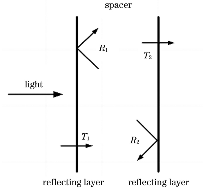
    Fig. 1. F-P film structure diagram
    Optical constant curves of two materials. (a) SiO2; (b) Ta2O5
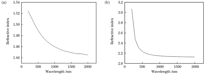
    Fig. 2. Optical constant curves of two materials. (a) SiO2; (b) Ta2O5
    Design curve of the film system
    Fig. 3. Design curve of the film system
    Structure diagram of optical film thickness monitoring system
    Fig. 4. Structure diagram of optical film thickness monitoring system
    SiO2 film monitoring curve
    Fig. 5. SiO2 film monitoring curve
    Surface roughness changes before and after coating at different rates. (a) Ta2O5; (b) SiO2
    Fig. 6. Surface roughness changes before and after coating at different rates. (a) Ta2O5; (b) SiO2
    Variations of film surface roughness under different ion source energies. (a) Ta2O5; (b) SiO2
    Fig. 7. Variations of film surface roughness under different ion source energies. (a) Ta2O5; (b) SiO2
    Test spectral curve of the filter film
    Fig. 8. Test spectral curve of the filter film
    Spectral curve of 44-layer dual-chamber membrane system
    Fig. 9. Spectral curve of 44-layer dual-chamber membrane system
    Influence of thickness change of Ta2O5 on spectral curve of the film system. (a) Relative thikness of Ta2O5 is 0.9; (b) relative thickness of Ta2O5 is 0.95; (c) relative thickness of Ta2O5 is 1.05; (d) relative thickness of Ta2O5 is 1.1
    Fig. 10. Influence of thickness change of Ta2O5 on spectral curve of the film system. (a) Relative thikness of Ta2O5 is 0.9; (b) relative thickness of Ta2O5 is 0.95; (c) relative thickness of Ta2O5 is 1.05; (d) relative thickness of Ta2O5 is 1.1
    Influence of SiO2 thickness change on spectral curve of the film system. (a) Relative thickness of SiO2 is 0.9; (b) relative thickness of SiO2 is 0.95; (c) relative thickness of SiO2 is 1.05; (d) relative thickness of SiO2 is 1.1
    Fig. 11. Influence of SiO2 thickness change on spectral curve of the film system. (a) Relative thickness of SiO2 is 0.9; (b) relative thickness of SiO2 is 0.95; (c) relative thickness of SiO2 is 1.05; (d) relative thickness of SiO2 is 1.1
    Debugging flow chart
    Fig. 12. Debugging flow chart
    Relative sensitivity of each film layer in the film system
    Fig. 13. Relative sensitivity of each film layer in the film system
    Spectral curve after improvement
    Fig. 14. Spectral curve after improvement
    ParameterIndicator
    Central wave length /nm1304.58
    Angle of incidence /(°)5.4
    Passband /nm2.2
    Ripple within passband /dB≤0.2
    Maximum insertion loss within passband /dB≤0.2
    Reflection band /nm1260-(λc-3.2)&(λc+3.2)-1360
    Reflection isolation within passband /dB>27
    Thickness /mm<0.8
    Table 1. Technical requirements for optical communication filter films
    MaterialBeam voltage /VBeam current /mAAccelerating voltage /VAngle /(°)E/B

    O2 flow in gas tube 1/

    (mL·min-1

    Ar flow in gas tube 2/

    (mL·min-1

    Ar folw in gas tube 3/

    (mL·min-1

    Ta2O51150950600141.55008
    SiO21150950600141.55008
    Table 2. Ion source parameters
    Material

    Rate /

    (nm·s-1

    Temperature /℃Hearth speed /(r·min-1

    Flow /

    (mL·min-1

    Dome speed /

    (r·min-1

    DomeMonitorWall
    Ta2O50.42002001501/100030180
    SiO20.82002001501/5000180
    Table 3. Process parameters of two materials
    Jing Zhang, Haicheng Liu, Xiuhua Fu, Shengqi Wang, Yibo Wang, Junqi Liu, Tianxiang Zhang, Fei Yang, Gang Li. Development of LWDM Narrow‑Band Filter Membrane for 5G Communication[J]. Chinese Journal of Lasers, 2023, 50(19): 1903101
    Download Citation