
Pui-In Mak. Lab-on-CMOS — an in-vitro diagnostic (IVD) tool for a healthier society[J]. Journal of Semiconductors, 2020, 41(11): 110301
- Journal of Semiconductors
- Vol. 41, Issue 11, 110301 (2020)
Abstract
What is in-vitro diagnostic (IVD) tool?
The failure of healthcare services is largely associated with the lack of proper equipment for diagnosis. The pandemic of COVID-19 signifies once again the leak of low-cost easy-to-use point-of-care diagnostic tools suitable for self-assessment when the people have unobvious symptoms. Delays in screening and treatment not only worsen the situation of individuals, but also the communities for heavily contagious diseases. An easy-to-use and comfortable diagnostic tool is also the key to encourage the participation of kids and elderly people. Especially for deadly contagious diseases like COVID-19, the turnaround time strongly affects their level of transmission to the community. An ideal in-vitro diagnostic (IVD) tool should be very low cost, easy to use, tiny sample consumption from the human body (e.g. blood, urine, sputum and tissue), and provide accurate result in a short time.
What is lab-on-CMOS IVD tool?
CMOS biosensors can underpin a number of transducing mechanisms (e.g. impedance, fluorescence, and nuclear spin) suitable for a wide variety of biological/chemical detection such as DNA, protein and bacteria/cells. A high-sensitivity biosensor allows a tiny specimen consumption, which can sit directly on the chip surface for direct reading and actuation by the readout circuitry underneath. A typical readout circuitry consists of an analog front-end (e.g. low-noise amplifier and filter) for signal conditioning, an analog-to-digital converter for digitization, and a digital back-end for signal processing. The final diagnostic result can be collected offline by reading the on-chip memory, or online via an on-chip wireless radio (Bluetooth). The overall technology goal is to achieve sample-in result-out diagnosis with minimum cost and human intervention.
IVD tool markets
According to a report by the World Health Organization (WHO), the leading infectious diseases (lower respiratory infections, HIV/AIDS, diarrhoeal diseases, malaria, and tuberculosis) account for roughly one-third of all deaths in low-income countries. Also the strong growth in population in these areas gives rise to the demand for affordable IVD tools. A forecast of the global IVD market will grow from USD 68.12 billion in 2018 to USD 87.93 billion by 2023.
Case study — nuclear magnetic resonance (NMR) for biological/chemical assays in CMOS
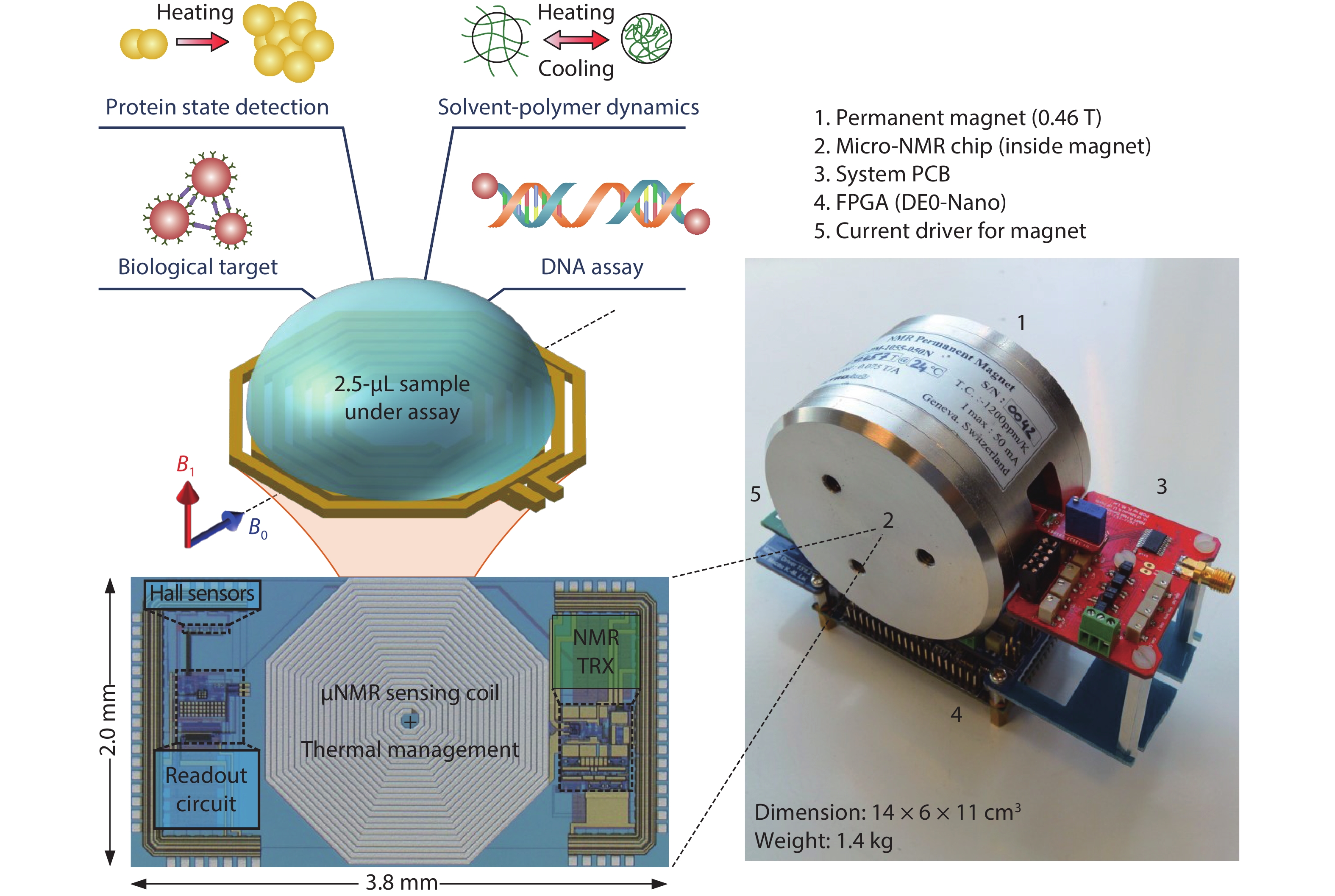
An example of our previous works is a handheld nuclear magnetic resonance (NMR) CMOS platform for multi-type biological/chemical assays, as depicted in Fig. 1. It mainly consists of a palm-size magnet (0.46 T, 1.25 kg) for nucleus magnetization and a transceiver chip fabricated in 0.18 μm CMOS. With an on-chip spiral coil, a micro-liter droplet sample can sit on the chip surface for direct measurement. Other key components are a system PCB for I/O interface, an FPGA for system control, a current driver for trimming the magnetic field of the magnet. The transceiver chip also integrated a current-mode vertical Hall sensor and a low-noise readout circuit to facilitate closed-loop B-field stabilization, as shown in Fig. 2, which otherwise fluctuates with temperature or sample displacement. The entire system achieves: 1) selective biological target pinpointing; 2) protein state analysis; and 3) solvent-polymer dynamics, suitable for healthcare, food and colloidal applications, respectively. Compared to a commercial NMR-assay product (Bruker mq-20), this platform greatly reduces the sample consumption (120×), hardware volume (175×), and weight (96×). With this experience, the author is currently investigating a low-cost portable magnetic resonance imaging (MRI) technology for diagnostic and therapeutic purpose such as diagnosis of anterior cruciate ligament tears, inflammation and tumors.
![]()
Figure 1.(Color online) A handheld NMR CMOS platform: (left) chip photo and its applications for multi-type assays, and (right) platform assembly. Courtesy K.M. Lei ISSCC 2016.
![]()
Figure 2.(Color online) System block diagram of the NMR transceiver. The transmitter and receiver transduce between magnetic and electrical signals with a thermal-controlled spiral coil. The
Opportunities and challenges
To leap up the possibility of lab-on-CMOS diagnosis (e.g. one-sample-in multiple-result-out), the fusion of multi-type CMOS biosensors-on-a-chip is prospective. We also can take advantages of post-processing after chip manufacturing such as chemical deposition and micromachining to raise the versatility and sensitivity of the CMOS biosensors. However, researchers/engineers having a multidisciplinary research background are hard to train/find, but their presence in a team will certainly boost up the creativity level for solving the unconventional problems in a smart way. This argument inspires that our education model for microelectronics should be broadened to include cross-disciplinary subjects in the syllabus. On the other hand, multiphysics software tools have enabled co-design between the biosensors and analog interfaces for years, but it is rare to see a simulation software for chemistry research with multiphysics and electronics. A successful one will play a key role in performance prediction and implementation of advanced lab-on-CMOS systems. In overall, the opportunities and challenges fairly come together in this synergy of electronic engineering, material sciences, biology and chemistry. Are we ready for a new era of the talent education system?
References

Set citation alerts for the article
Please enter your email address
© Copyright 2018-2021 | Chinese Laser Press. All Rights Reserved 沪ICP备15018463号-20