• Chinese Optics Letters
  • Vol. 20, Issue 9, 090501 (2022)
Guoqing Ma1、2, Changhe Zhou1、2, Yongfang Xie3, Ge Jin3, Rongwei Zhu1、2, Jin Zhang1, Junjie Yu1、2、*, and Guohai Situ1、2、**
Author Affiliations
  • 1Laboratory of Information Optics and Optoelectronic Technology, Shanghai Institute of Optics and Fine Mechanics, Chinese Academy of Sciences, Shanghai 201800, China
  • 2Center of Materials Science and Optoelectronics Engineering, University of Chinese Academy of Sciences, Beijing 100049, China
  • 3Institute of Photonics Technology, Jinan University, Guangzhou 510000, China
  • show less
    DOI: 10.3788/COL202220.090501 Cite this Article Set citation alerts
    Guoqing Ma, Changhe Zhou, Yongfang Xie, Ge Jin, Rongwei Zhu, Jin Zhang, Junjie Yu, Guohai Situ. Double-groove rectangular gratings for high-efficiency wideband vertical coupling in planar-integrated optical systems[J]. Chinese Optics Letters, 2022, 20(9): 090501 Copy Citation Text show less

    Abstract

    A planar-integrated optical system (PIOS) represents powerful optical imaging and information processing techniques and is a potential candidate for the realization of a three-dimensional (3D) integrated optoelectronic intelligent system. Coupling the optical wave carrying information into a planar transparent substrate (typically fused silica) is an essential prerequisite for the realization of such a PIOS. Unlike conventional grating couplers for nano-waveguides on the silicon-on-insulator platform, the grating couplers for PIOS enable to obtain a higher design freedom and to achieve much higher coupling efficiency. By combining the rigorous coupled wave algorithm and simulated annealing optimization algorithm, a high-efficiency asymmetric double-groove grating coupler is designed for PIOS. It is indicated that, under the condition of the normal incidence of TE polarization, the diffraction efficiency of the -1st order is over 95%, and its average value is 97.3% and 92.8% in the C and C+L bands. The simulation results indicate that this type of grating coupler has good tolerance and is expected to be applied in optical interconnections, waveguide-based augmented reality glasses, and planar-integrated 3D interconnection optical computing systems.

    1. Introduction

    Optical computing has again garnered significant attention in the past few years, due to its potentials in addressing the barriers and challenges in computing power and energy efficiency encountered by conventional electronic processors in the post Moore era[14]. Benefitting from its good compatibility with standard complementary metal-oxide-semiconductor (CMOS) technology, the optical computing scheme based on planar nano-waveguide systems on the silicon-on-insulator (SOI) platform, referred to as nanophotonic integrated circuits, has advanced substantially, especially after Shen’s work in 2017[5]. However, in this scheme, one must rearrange the input two-dimensional (2D) matrix into a one-dimensional (1D) vector to match with the 1D port array of nano-waveguides[6,7]. Compared with nanophotonic integrated circuits, it is possible for the three-dimensional (3D) interconnected solutions[812] to directly process the input 2D optical signals (especially for input images) without conventional optical-electrical/electrical-optical conversion. In addition, the 3D interconnected solution can fully utilize the inherent massive parallelism in optics to directly realize the 2D-matrix-to-2D-matix multiply-accumulation operation (MAC), leading to unprecedented computational capability compared to their electric counterparts. A planar-integrated optical system (PIOS)[1315] is an effective integrated way to realize the 3D interconnected solutions, where a given free-space optical system is tilted and folded into a planar transparent substrate, and various diffractive optical elements are used to realize the functions such as a lens for realizing light modulation. Therefore, this integration into a planar substrate makes PIOSs mechanically stable and robust and protects the optical path against airflow disturbances, similar to the nanophotonic integrated circuit. In this integrated solution, the high-efficiency coupling of external optical signals into the planar substrate is an important prerequisite for the realization of 3D integrated optoelectronic intelligence systems. Generally, the coupling solutions are mainly divided into two categories: the end-face and surface couplers. The main disadvantage of end-face coupling is that high coupling efficiency is difficult to achieve on a large scale, such as 64×64, 128×128, and 256×256. The surface couplers mainly realize the coupling through micro/nano-artificial structures, such as subwavelength gratings, and the angle of the transmitted light is altered by the diffraction to meet the condition of total internal reflection of the substrate. In conventional nanophotonic integrated circuits, various grating couplers were used for coupling light from a fiber into a planar nano-waveguide[1618], where the grating etching depth should be no more than the thickness of the waveguide, and the material within the grating region and the grating size are also limited for a standard SOI platform. Compared with those conventional nano-waveguide grating couplers, the grating couplers for PIOSs offer more design freedom, and thus it is possible to achieve a much higher coupling efficiency. Recently, with the renaissance of augmented reality (AR) and virtual reality (VR) technologies, this type of grating coupler is also garnering a lot of attention[19].

    Currently, the grating couplers for planar substrates are mainly realized by blazed or slanted gratings. The utilization of blazed gratings is the most straightforward choice to realize the deflection of light. However, for conventional blazed gratings, the deflection angle is generally not large enough, and the coupling efficiency is also not very high (typically 84%)[20]. Although this can be somewhat circumvented by blazed binary gratings when the period is much smaller than the working wavelength, the subwavelength binary grating typically has a small feature size (the minimum line width) and a high aspect ratio in order to achieve high efficiency[21,22]. On the other hand, the slanted grating working in the resonant domain is another choice to realize these couplers. However, to fabricate slanted gratings, a special etching process and specially designed devices are also required. The typical coupling efficiency is only 90% for the slanted gratings fabricated in practice[23]. Moreover, the slanted grating is also not appropriate for massive replication because of its slanted ridge, especially for gratings with a large slanted angle. Most conventional grating couplers are usually realized by their single-groove grating structure. Compared with single-groove gratings, the double-groove structure provides more degrees of freedom for the design, and these double-groove gratings tend to have a higher performance. Therefore, the double-groove gratings have been widely investigated in the past decades and designed for the realization of various filters[24], polarizers[25], beam splitters[26], high-efficiency gratings used in Littow mounting[27], enhanced light trapping[28], gas pressure detection[29], etc. Among them, the grating coupler realized by double-groove gratings in the resonant domain has been an interesting topic for years. In 2006, Laakkonen et al. theoretically introduced a type of double-groove, two-depth grating for high-efficiency light coupling into a light guide, where light diffracted into the first order that is deflected at an angle greater than the angle of total reflection is coupled[30]. However, this structure requires the aspect ratio (defined as the ratio of etching depth to feature size) to be greater than 7.8 for TE and 16 for TM polarization. In addition, this two-depth grating has two different etching groove depths, and thus usually requires the troublesome multi-step lithography technique[31]. In 2010, Iizuka et al. numerically demonstrated a double-groove grating coupler operating at a wavelength of 600 nm under normal incidence by the modal method[32]. It was indicated that the theoretical diffraction efficiency was up to 96.9% with a deflection angle of 50°. However, the normalized feature size (defined as the feature size normalized by the working wavelength) of this coupler was only 0.058, and the aspect ratio was as large as eight, making this grating structure very challenging to manufacture. Four years later, Matsui et al. re-optimized and designed a double-groove grating coupler with a period of 580 nm operating at a wavelength of 640 nm based on a similar grating structure. The normalized feature size was increased to 0.0938, and the aspect ratio was reduced to 3.8, at the cost of lower coupling efficiency. The theoretical efficiency was approximately 88.9%, whereas the actual diffraction efficiency of this grating coupler was only 70% in the experiment[33].

    In this study, a high-efficiency broadband grating coupler for vertical coupling based on an asymmetric double-groove structure is designed using the rigorous coupled wave algorithm (RCWA) and simulated annealing (SA) algorithm. The asymmetric structure allows perfect vertical fiber coupling, resulting in less difficulties in alignment and packaging, less angle dependence, and denser integration. It is indicated that the average coupling efficiency of the 1st order is up to 97.3% in the C band for TE polarization, and the corresponding deflection angle of the 1st order ranges from 46.24° to 47.59°, which is larger than the critical angle between the substrate and covering air. Therefore, such a large deflection angle allows the 1st order to propagate within the substrate because of the total internal reflection effect, and this integration provides 3D interconnection capability and also protects the optical path against airflow disturbances. Moreover, the normalized feature size is 0.0948 (corresponding to 150nm), and the aspect ratio is 4.2. In addition, the tolerance analysis suggests that the lateral error of the most sensitive ridge and groove width is about 10 nm, and the vertical error of the most sensitive etching depths is 12 nm, which could be well achieved by the standard electron-beam (e-beam) lithography and plasma-based dry etching technologies. The grating coupler designed in this study could be used for PIOS-based integrated optoelectronic intelligence systems, such as new devices for optical interconnection and all-optical computing accelerators, which can avoid the limitation of optical-electric/electric-optical conversion, making it possible to directly couple the 2D array optical signals into the substrate waveguide layer for all-optical signal processing.

    2. Design Consideration and Optimization Model

    2.1. Design consideration

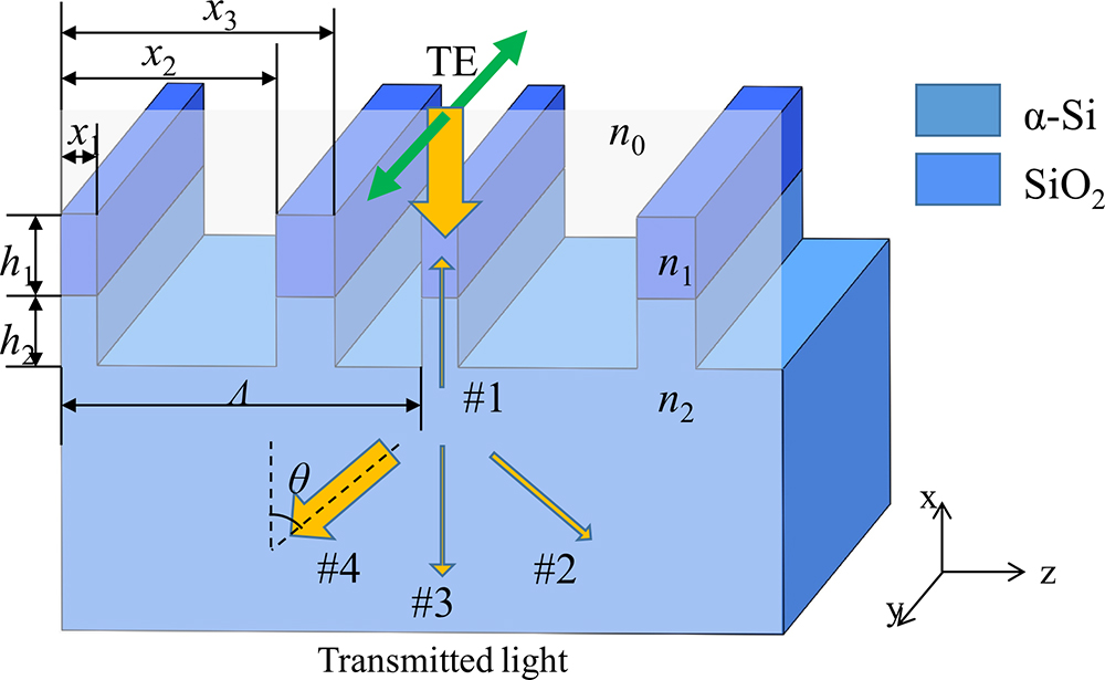
    Figure 1 illustrates the structure diagram of the asymmetric double-groove grating coupler. A TE-polarized plane wave is normally incident from top to bottom. The cover medium is air, and the refractive index of n0 is 1.0. There are two ridge layers within the grating region: the first layer is a high-refractive-index (n1) ridge layer, and the second is a low-refractive-index (n2) ridge layer that is similar to the substrate. In contrast to classical gratings, there are two ridges in one period for this asymmetric double-groove grating coupler. Within one period, the actual positions of the two ridges are x1, x2, and x3, and the grating period is Λ. Then, the width of the first ridge is w1=x1, the width of the second ridge is w3=x3x2, and the groove width between these two ridges is w2=x2x1. To achieve high-efficiency coupling, the 1st (port #4) order is chosen as the working order; thus, the transmitted light field will be dominantly coupled into the 1st order. To achieve high mode coupling efficiency, the grating ridge is chosen as the material with high refractive index in the working waveband[3133]. In addition, the ridge and substrate should be as transparent as possible to reduce absorption loss. Here, the first ridge layer is chosen as silicon (α-Si, Pierce and Spicer, 1972[34]) with a thickness of h1 and refractive index of n1=3.48 at the central wavelength of 1550 nm, and the second ridge layer is selected as fused silica (SiO2) with a thickness of h2 and refractive index of n2=1.444.

    Schematic diagram of the grating coupler based on the double-groove structure. The green arrow represents the polarization direction, port #1 represents the reflective 1st order, and ports #2, #3, and #4 represent the transmitted +1st, 0th, and −1st orders, respectively.

    Figure 1.Schematic diagram of the grating coupler based on the double-groove structure. The green arrow represents the polarization direction, port #1 represents the reflective 1st order, and ports #2, #3, and #4 represent the transmitted +1st, 0th, and −1st orders, respectively.

    According to the analysis results of the mode coupling theory[30,32,33], the incident plane wave could excite only three orthogonal modes within the grating region when the period is small enough. Therefore, we limit the relative period Λ/λ to allocate the diffraction energy into the +1st (port #2) or 1st (port #4) order as much as possible, according to the following grating equation: n2sinθm+sinθin=mλΛ,where n2 is the refractive index of the substrate material, θm is the diffraction angle for the mth order, θin is the incident angle with m being the diffraction order, Λ is the grating period, and λ is the incident wavelength. By limiting the relative period Λ/λ, the diffraction angle of high diffraction orders (m2) exceeds 90°, resulting in evanescent waves. Thus, the energy diffracted by the grating is dominantly allocated to low diffraction orders whose diffraction angles are less than 90°. Therefore, we set the relative period to satisfy the relationship of 0.69<Λ/λ<1.38 under the condition of θin=0°, and n2=1.444 at a central wavelength of λ=1550nm. Furthermore, according to the grating equation expressed in Eq. (1), the diffraction angles of the finally transmitted ±1st order are larger than the critical angle of total internal reflection at the substrate–air interface when the Λ is smaller than λ. In this case, the transmission of light will be restrained into the substrate and propagated along zigzag paths inside the substrate waveguide[3537]. Therefore, we set the relative period 0.69<Λ/λ<1 to further reduce the searching scope. Under this condition, only four propagating diffraction orders remain, including the transmitted ±1st (ports #2 and #4), 0th (port #3) orders, and the reflective 0th (port #1) order. By adopting the asymmetric double-groove grating structure, the mode profile within the grating region will become asymmetric. Thus, it is possible to dominantly concentrate the light energy into the 1st order, and only a little energy is coupled into the +1st and 0th orders.

    2.2. Optimization model

    Based on the above discussions, the RCWA method[38,39] combined with the SA algorithm is employed in this study to search the structure parameters of the grating coupler. In this model, six structure parameters are chosen as the searching variables, including three positions of those two ridges, i.e., x1, x2, x3 with constraints of 0<x1<x2<x3<Λ, the depths of two ridge layers, h1 and h2, and the grating period 0.69<Λ/λ<1. To constrain the energy into the 1st order, the diffraction efficiencies of the 1st and +1st orders should be maximized and minimized, respectively, at the same time. Notice that the 0th order will pass through the substrate and not cause any noise inside the substrate waveguide; thus, the 0th order does not need to be minimized for this configuration. The cost function is written as fcost(x1,x2,x3,h1,h2,Λ)=λlλu{C1×[ηTE1(λ)1]2+C2×[ηTE1(λ)]2}dλ+(1C1C2)hwmin,where C1 and C2 are weight coefficients, and ηTE1 and ηTE1 are the diffraction efficiencies of the 1st and +1st orders for TE polarization. The total ridge depth is h=h1+h2, and the feature size is defined as wmin=min(x1,x2x1,x3x2,Λx3). By maximizing the diffraction efficiency of the 1st order, minimizing that of the +1st order, and minimizing the ratio of total ridge depth to feature size, one can obtain the optimized structure parameters of the double-groove grating coupler. During optimization, the weight coefficients could be adjusted to achieve a trade-off between the grating performance (diffraction efficiencies) and fabrication difficulty (feature size and aspect ratio).

    3. Results and Discussions

    The final optimization results of the six structure parameters in the C and C+L bands are presented in Table 1. It is evident that the grating period is Λ=1.467µm for the C band and Λ=1.476µm for the C+L band, which are slightly smaller than the operating wavelength. In the C band, the first ridge width is w1=147nm, the second ridge width is w3=236nm, and the groove width between them is w2=726nm, with a feature size of wmin=147nm. The depths of the first ridge layer (α-Si) and the second layer (SiO2) are h1=331nm and h2=290nm, and the aspect ratio is 4.24. In the C+L band, w1=148nm, w2=241nm, and w3=745nm, with feature size of wmin=148nm. The depths of the two ridge layers are h1=341nm and h2=290nm, and the aspect ratio is 4.26. The optimized grating parameters of two grating couplers are similar, and their average coupling efficiencies at the 1st order are 97.3% and 92.8% in the C and C+L bands, respectively.

    Bandh1 (µm)h2 (µm)x1 (µm)x2 (µm)x3 (µm)Λ (µm)ηTE1 (%)ηTE1 (%)
    C (1535–1565 nm)0.3310.290.1470.8731.1091.46797.31.5
    C+L (1535–1625 nm)0.3410.270.1480.8931.1371.47692.81.6

    Table 1. Structure Parameters and Diffraction Efficiencies of Two Double-Groove Grating Couplers Optimized for TE Polarization Working in the C and C+L Bands, Respectively

    Furthermore, we simulated the electric field distribution based on the finite element method (FEM), when a collimated Gaussian beam from a single-mode fiber with a collimation lens is normally incident on the grating coupler with TE polarization. Here, the waist radius of the collimated Gaussian beam is 75 µm with a monochromatic wavelength of 1550 nm, and the incident electric field power is 1 V/m. The upper and lower boundary conditions of the substrate are defined as impedance boundary conditions, and other boundary conditions are defined as scattering boundary conditions. A self-adaptive triangular mesh is selected, and the maximum mesh size is 200 nm. The simulation results illustrated in Fig. 2 clearly indicate that light energy is dominantly coupled into the 1st order, and the electric field along the 1st order is reflected by sandwiching the substrate with the top and bottom substrate–air interfaces, owing to the total internal reflection effect. As expected, the light field dominantly propagates along the zigzag path, and the path is folded inside the substrate; thus, this configuration enables the integration of the 3D free-space light propagation. Also, it is evident that the diffractive angle of the 1st order is approximately 47°, which is very close to the theoretical value of θ=47.02°. The inset (in the red box) in Fig. 2 illustrates a partially enlarged electric field distribution within the grating region, which indicates the entire picture of the light field diffraction of the grating under normal incidence. It can be observed that the intensity of the light field is manifested with high asymmetry, and the incident Gaussian field is dominantly coupled into asymmetric grating modes because of this double-groove structure.

    Simulation results of the electric field inside the substrate with the double-groove grating coupler when the Gaussian wave from a single-mode fiber is normally incident with TE polarization. The inset (in the red box) is the enlarged electric field distribution within the grating region.

    Figure 2.Simulation results of the electric field inside the substrate with the double-groove grating coupler when the Gaussian wave from a single-mode fiber is normally incident with TE polarization. The inset (in the red box) is the enlarged electric field distribution within the grating region.

    In addition, the diffraction efficiency versus the wavelength is investigated further. As illustrated in Fig. 3(a), the diffraction efficiency of the 1st order for TE polarization under a condition of normal incidence always exceeds 95% in the C band (1530–1565 nm), and its average diffraction efficiency is up to 97.3%. As illustrated in Fig. 3(b), the coupling efficiency is over 85% in the entire C+L band (1530–1625 nm), and the corresponding average efficiency is 92.8%. In addition, it is observed from both Figs. 3(a) and 3(b) that when the illumination wavelength is deviated from the central wavelength, the efficiency of the +1st order is always kept low enough (<2%), and the energy is mainly transferred to the 0th order, which will pass through the substrate and does not induce any noise. From Fig. 3(c), it is quite evident that the incident plane wave is normally incident (the propagation direction is perpendicular to the wave front), and the transmitted field is mainly coupled into the 1st order. Notwithstanding the results obtained by RCWA, we also adopted FEM to calculate the diffraction efficiency curve for verification. It is indicated that those results are well consistent with those obtained by the RCWA method. In addition, we also extracted the parameters of the electric field calculated by FEM, and the rigorous result of the diffraction angle of the 1st order was θ=47.02°, which is in perfect agreement with that obtained by RCWA. This result indicated that the diffraction angle is larger than the critical angle θc=arcsin(nair/n2)=43.8° of the substrate–air interface, which again verified the expectation of the light propagating inside the substrate. Further, the total transmission energy of the ±1st and 0th orders at 1550 nm is approximately 99.8%, which indicates that approximately all incident energy is transmitted into the substrate, and the reflected energy is negligible. Further, the diffraction efficiency of the +1st order is smaller than 2% in Fig. 3(a), which suggests that light energy coupled into the +1st order is small enough, and the signal to noise ratio will be larger than 16.8 dB for the entire C band, even if all the light in the undesired +1st order is aliased with the signal.

    Relationship between the coupling efficiency calculated by the RCWA, SA algorithms as well as FEM, and the working wavelength λ (a) in the C band and (b) in the C+L band, and (c) electric field distribution diagram at the central wavelength of λ = 1550 nm.

    Figure 3.Relationship between the coupling efficiency calculated by the RCWA, SA algorithms as well as FEM, and the working wavelength λ (a) in the C band and (b) in the C+L band, and (c) electric field distribution diagram at the central wavelength of λ = 1550 nm.

    4. Tolerance Analysis

    In the manufacturing process of the grating coupler, the actual shape of the grating structure always deviates from optimized parameters because of various fabrication errors, resulting in the deterioration in performances, such as coupling efficiency, and light noises at other undesired orders of the grating coupler. Therefore, it is necessary to assess the manufacturing tolerances of the grating design. In this section, we have selected several important structure parameters of the grating coupler for tolerance investigation.

    When other parameters are fixed and equal to the optimized parameters, the influence of each parameter, including the grating period Λ, lateral positions of two ridges x1, x2, x3, and two depths h1 and h2, on the coupling efficiency of the 1st order is investigated in sequence, under the TE-polarized plane wave normal incidence, as illustrated in Figs. S1 and S2 in Supplementary Material. The broken rectangles and the dot rectangles denote the areas where the diffraction efficiency is higher than 90% in the C band and 80% in the C+L band.

    In the C band, it is observed from Fig. S1(a) in Supplementary Material that the grating period Λ can be changed from 1.44 µm to 1.49 µm. It is not difficult to control the grating period error within the nanometer range with the help of a laser interferometer[40], and this deviation in the grating period is far less than that tolerance. In Figs. S1(b)–S1(d) of Supplementary Material, the lateral positions, x1, x2, x3, vary from 125 nm to 155 nm, 867 nm to 882 nm, and 1102 nm to 1115 nm, and the coupling efficiencies are always over 90% in the C band, which indicates lateral tolerances of 30 nm, 15 nm, and 13 nm for these three positions, respectively. The position tolerances could be well achieved by advanced e-beam lithography. In addition, from Figs. S1(e) and S1(f) in Supplementary Material, it is evident that the diffraction efficiency always exceeds 90% in the C band, when h1 and h2 change from 323 nm to 340 nm with a tolerance of 17 nm and from 180 nm to 405 nm with a tolerance of 225 nm, respectively. The tolerance of 17 nm for the top α-Si layer should not be a challenge with a plasma-enhanced chemical vapor deposition method. Note that the tolerance of the second SiO2 layer is up to 225 nm, which is very beneficial for the grating fabrication, and this tolerance will be easy to achieve when a plasma-based dry etching technology is adopted. Furthermore, the difference in the depositing process of the thin films of α-Si and SiO2 often causes some deviation in the refractive index. Figures S3(a) and S3(b) in Supplementary Material illustrate the influence of the deviation in the refractive index of α-Si and SiO2 on the coupling efficiency of the 1st order. Practically, the derivation in the refractive index is far smaller than these tolerances. Further, we also investigate the tolerance of the incident angle. Figure S4(a) in Supplementary Material illustrates that diffraction efficiency is always more than 90% in the entire C band when the incident angle varies from 1.8° to +2.8°, and this deviation in the incident angle could be easy to achieve.

    In the C+L band, as shown in Fig. S2 in Supplementary Material, it is evident that a tolerance of 35 nm, 30 nm, 13 nm, 12 nm, 14 nm, and 265 nm is obtained for Λ, x1, x2, x3, and two depths h1, h2, respectively. In addition, Figs. S3(c) and S3(d) in Supplementary Material illustrate that the refractive index of Si and SiO2 is altered from 3.43 to 3.51 and from 1.29 to 1.67, respectively. As illustrated in Fig. S4(b) in Supplementary Material, it can be observed that the tolerance of the incident angle is approximately 4° (from 1° to 2.8°). Thus, the tolerance of the grating coupler working in the C+L band will be similar to that in the C band if the low level of coupling efficiency decreases from 90% to 80%. In order to assess the impact of more actual tolerance, we used the Monte Carlo method to simulate actual tolerances in those five structure parameters, including three lateral positions x1, x2, x3 and two depths h1, h2 of the designed grating couplers in the C band and C+L band, respectively. In each simulation, those structure parameters were randomly generated according to a Gaussian distribution within the range of their tolerance in Figs. S1 and S2 in Supplementary Material. We repeated 1000 times and calculated the corresponding average diffraction efficiency for each simulation, as shown in Fig. 4. One can see that the average efficiencies in the C and C+L bands are 94.4% and 91.2%, respectively.

    Simulation results of 1000 samples of the grating couplers based on the Monte Carlo method. The average efficiencies of the couplers in the (a) C and (b) C+L bands for these 1000 samples; statistical distributions of the efficiency of these 1000 samples in the (c) C and (d) C+L bands.

    Figure 4.Simulation results of 1000 samples of the grating couplers based on the Monte Carlo method. The average efficiencies of the couplers in the (a) C and (b) C+L bands for these 1000 samples; statistical distributions of the efficiency of these 1000 samples in the (c) C and (d) C+L bands.

    These analyses show that the proposed double-groove grating coupler has good tolerance, and these couplers should be realizable by standard e-beam lithography and plasma-based dry etching technologies. The coupling efficiency is far larger than that of the couplers in nano-waveguides, and the double-groove grating couplers could be used in the wideband. Moreover, note that the tolerance of the refractive index of two ridge layers, especially the second layer, is very large, which suggests that the derivation in the refractive index has little influence on the coupling efficiency. Therefore, it is expected to construct PIOS-based integrated optoelectronic intelligent systems based on different material systems.

    5. Conclusion

    Based on the RCWA and SA algorithm, a type of double-groove grating for high-efficiency wideband vertical coupling in PIOSs was designed. As examples, two double-groove gratings were designed for the C and C+L bands, respectively. The average coupling efficiency of the 1st was up to 97.3% in the C band and 92.8% for the C+L band under the condition of the TE-polarized normally incident plane wave. The results indicated that the diffraction angle of the 1st order of the grating coupler working in the C and C+L band ranged from 46.24° to 47.59° and 46.24° to 50.05°, respectively, which satisfies the total internal reflection condition in the SiO2/air interface. FEM was also adopted for numerical simulation, and the results agree well with those obtained by RCWA. Further, the simulation clearly demonstrated the way that the electric field propagates along the zigzag path inside the substrate, owing to the total internal reflection effect. In addition, the tolerance investigation on several key structure parameters of the grating coupler was also discussed. Furthermore, the tolerance errors in the incident angle and the deviation in the refractive index of materials were also investigated. It is worth noting that for the grating coupler designed here, the normalized feature size is 0.0948 (corresponding feature size is 150nm), and the aspect ratio is 4.2. Moreover, it is indicated that this type of grating coupler has good tolerance and can be fabricated by standard e-beam lithography combined with plasma-based dry etching technology. Compared with the slanted grating structure, the fabrication process of this double-groove rectangular grating coupler was easily compatible with standard CMOS technology. Moreover, this rectangular grating was also more appropriate to massively replicate through standard nano-imprinting technology[41,42]. In conclusion, the double-groove rectangular grating coupler enabled the integration of the 3D optical interconnect solution, and this type of planar-integrated optoelectronic intelligent computing system will be significant in all-optical information processing, which will fundamentally solve the predicament faced by the conventional electric circuit in the post Moore era. In addition, this grating coupler is expected to be practically utilized in AR/VR optical engines.

    References

    [1] M. A. Taubenblatt. Optical interconnects for high-performance computing. J. Light. Technol., 30, 448(2012).

    [2] G. Wetzstein, A. Ozcan, S. Gigan, S. Fan, D. Englund, M. Soljačić, C. Denz, D. Miller, D. Psaltis. Inference in artificial intelligence with deep optics and photonics. Nature, 588, 39(2020).

    [3] W. Bogaerts, D. Pérez, J. Capmany, D. Miller, J. Poon, D. Englund, F. Morichetti, A. Melloni. Programmable photonic circuits. Nature, 586, 207(2020).

    [4] C. Li, X. Zhang, J. Li, T. Fang, X. Dong. The challenges of modern computing and new opportunities for optics. PhotoniX, 2, 20(2021).

    [5] Y. Shen, N. Harris, S. Skirlo, M. Prabhu, T. Baehr-Jones, M. Hochberg, X. Sun, S. Zhao, H. Larochelle, D. Englund, M. Soljačić. Deep learning with coherent nanophotonic circuits. Nat. Photonics, 11, 441(2017).

    [6] J. Feldmann, N. Youngblood, M. Karpov, H. Gehring, X. Li, M. Stappers, M. Le Gallo, X. Fu, A. Lukashchuk, A. S. Raja, J. Liu, C. D. Wright, A. Sebastian, T. J. Kippenberg, W. H. P. Pernice, H. Bhaskaran. Parallel convolutional processing using an integrated photonic tensor core. Nature, 589, 52(2021).

    [7] B. Shastri, A. Tait, T. Lima, W. Pernice, H. Bhaskaran, C. Wright, P. Prucnal. Photonics for artificial intelligence and neuromorphic computing. Nat. Photonics, 15, 102(2021).

    [8] X. Lin, Y. Rivenson, N. T. Yardimci, M. Veli, M. Jarrahi, A. Ozcan. All-optical machine learning using diffractive deep neural networks. Science, 361, 1004(2018).

    [9] T. Zhou, L. Fang, T. Yan, J. Wu, Y. Li, J. Fan, H. Wu, X. Lin, Q. Dai. In situ optical backpropagation training of diffractive optical neural networks. Photonics Res., 8, 940(2020).

    [10] T. Zhou, X. Lin, J. Wu, Y. Chen, H. Xie, Y. Li, J. Fan, H. Wu, L. Fang, Q. Dai. Large-scale neuromorphic optoelectronic computing with a reconfigurable diffractive processing unit. Nat. Photonics, 15, 367(2021).

    [11] A. Ryou, J. Whitehead, M. Zhelyeznyakov, P. Anderson, C. Keskin, M. Bajcsy, A. Majumdar. Free-space optical neural network based on thermal atomic nonlinearity. Photonics Res., 9, B128(2021).

    [12] D. Pierangeli, G. Marcucci, C. Conti. Photonic extreme learning machine by free-space optical propagation. Photonics Res., 9, 1446(2021).

    [13] G. Matthias, J. Jürgen, S. Stefan. Planar-integrated optical vector-matrix multiplier. Appl. Opt., 39, 5367(2000).

    [14] M. Gladys, G. Matthias, J. Jürgen, L. Jesús. Achromatic optical Fourier transformer with planar-integrated free-space optics. Appl. Opt., 44, 229(2005).

    [15] R. Heming, L. Wittig, P. Dannberg, J. Jahns, E. Kley, M. Gruber. Efficient planar-integrated free-space optical interconnects fabricated by a combination of binary and analog lithography. J. Light. Technol., 26, 14(2008).

    [16] H. Ma, H. Yang, B. Tang, M. Wei, J. Li, J. Wu, P. Zhang, C. Sun, L. Li, H. Lin. Passive devices at 2 µm wavelength on 200 mm CMOS-compatible silicon photonics platform [Invited]. Chin. Opt. Lett., 19, 071301(2021).

    [17] R. Ge, H. Li, Y. Han, L. Chen, J. Xu, M. Wu, Y. Li, Y. Luo, X. Cai. Polarization diversity two-dimensional grating coupler on x-cut lithium niobate on insulator. Chin. Opt. Lett., 19, 060006(2021).

    [18] N. Hoppe, W. Zaoui, L. Rathgeber, Y. Wang, R. Klenk, W. Vogel, M. Kaschel, S. Portalupi, J. Burghartz, M. Berroth. Ultra-efficient silicon-on-insulator grating couplers with backside metal mirrors. IEEE J. Quantum Electron., 26, 0001801(2020).

    [19] J. Xiong, E. Hsiang, Z. He, T. Zhan, S. Wu. Augmented reality and virtual reality displays: emerging technologies and future perspectives. Light Sci. Appl., 10, 216(2021).

    [20] M. Tian, M. Qu, L. Wu, X. Cheng. Progress on asymmetrical grating couplers for vertical coupling. Laser Optoelectron. Prog., 58, 0500004(2021).

    [21] J. N. Mait, D. W. Prather, M. S. Mirotznik. Design of binary subwavelength diffractive lenses by use of zeroth-order effective-medium theory. J. Opt. Soc. Am. A, 16, 1157(1999).

    [22] J. Xu, S. Yang, L. Wu, L. Xu, Y. Li, R. Liao, M. Qu, X. Quan, X. Cheng. Design and fabrication of a high-performance binary blazed grating coupler for perfectly perpendicular coupling. Opt. Express, 29, 42999(2021).

    [23] .

    [24] Y. Ding, R. Magnusson. Resonant leaky-mode spectral-band engineering and device applications. Opt. Express, 12, 5661(2004).

    [25] L. Sun, Z. Lv, W. Wu, W. Liu, J. Yuan. Double-grating polarizer for terahertz radiation with high extinction ratio. Appl. Opt., 49, 2066(2010).

    [26] J. Wu, C. Zhou, H. Cao, A. Hu, J. Yu, W. Sun, W. Jia. Beam splitting of a double-groove fused-silica grating under normal incidence. J. Opt., 13, 115703(2011).

    [27] K. Ito, H. Lizuka. Highly efficient -1st-order reflection in Littrow mounted dielectric double-groove grating. AIP Adv., 3, 062119(2013).

    [28] J. Wu. Enhanced light trapping with double-groove grating in thin-film amorphous silicon solar cells. Opt. Laser Tech., 79, 95(2016).

    [29] Y. Liu, J. Feng, Z. Li, J. Luo, T. Kou, S. Yuan, M. Li, Y. Liu, Y. Peng, S. Wang. Double-groove terahertz chirped grating waveguide tube for gas pressure detection. Laser Phys. Lett., 16, 056202(2019).

    [30] P. Laakkonen, S. Siitonen, M. Kuittinen. Double-groove, two-depth grating coupler for light guides. J. Opt. Soc. Am. A., 23, 3156(2006).

    [31] M. Oliva, D. Michaelis, T. Benkenstein, J. Dunkel, J. Harzendorf, A. Matthes, U. D. Zeitner. Highly efficient three-level blazed grating in the resonance domain. Opt. Lett., 35, 2774(2010).

    [32] H. Iizuka, N. Engheta, H. Fujikawa, K. Sato, Y. Takeda. Role of propagating modes in a double-groove grating with a +1st-order diffraction angle larger than the substrate–air critical angle. Opt. Lett., 35, 3973(2010).

    [33] T. Matsui, A. Miura, N. Ikeda, H. Fujikawa, Y. Sugimoto, N. Engheta, H. Iizuka. Experimental investigation of double-groove grating satisfying total internal reflection condition. Opt. Express., 22, 25362(2014).

    [34] D. T. Pierce, W. E. Spicer. Electronic structure of amorphous Si from photoemission and optical studies. Phys. Rev. B, 5, 3017(1972).

    [35] T. Levola. Diffractive optics for virtual reality displays. J. Soc. Inf. Disp., 14, 467(2006).

    [36] H. Mukawa. A full-color eyewear display using planar waveguides with reflection volume holograms. J. Soc. Inf. Disp., 17, 185(2009).

    [37] Z. Liu, C. Pan, Y. Pang, Z. Huang. A full-color near-eye augmented reality display using a tilted waveguide and diffraction gratings. Opt. Commun., 431, 45(2019).

    [38] M. G. Moharam, T. K. Gaylord. Rigorous coupled-wave analysis of planar-grating diffraction. J. Opt. Soc. Am., 71, 811(1981).

    [39] M. G. Moharam, Eric B. Grann, Drew A. Pommet, T. K. Gaylord. Formulation for stable and efficient implementation of the rigorous coupled-wave analysis of binary gratings. J. Opt. Soc. Am. A, 12, 1068(1995).

    [40] X. Xiang, M. Li, C. Wei, C. Zhou. Precision fringe period metrology using an LSQ sine fit algorithm. Appl. Opt., 57, 4777(2018).

    [41] W. C. Chuang, C. T. Ho, W. C. Wang. Fabrication of a high-resolution periodical structure using a replication process. Opt. Express, 13, 6685(2005).

    [42] K. J. Byeon, H. Lee. Recent progress in direct patterning technologies based on nano-imprint lithography. EPJ Appl. Phys., 59, 10001(2012).

    Guoqing Ma, Changhe Zhou, Yongfang Xie, Ge Jin, Rongwei Zhu, Jin Zhang, Junjie Yu, Guohai Situ. Double-groove rectangular gratings for high-efficiency wideband vertical coupling in planar-integrated optical systems[J]. Chinese Optics Letters, 2022, 20(9): 090501
    Download Citation