• Photonics Research
  • Vol. 6, Issue 5, 468 (2018)
Michael L. Davenport*, Songtao Liu, and John E. Bowers
Author Affiliations
  • Department of Electrical and Computer Engineering, University of California, Santa Barbara, California 93106, USA
  • show less
    DOI: 10.1364/PRJ.6.000468 Cite this Article Set citation alerts
    Michael L. Davenport, Songtao Liu, John E. Bowers. Integrated heterogeneous silicon/III–V mode-locked lasers[J]. Photonics Research, 2018, 6(5): 468 Copy Citation Text show less
    Schematic of the most common forms of fully integrated mode-locked laser cavity designs.
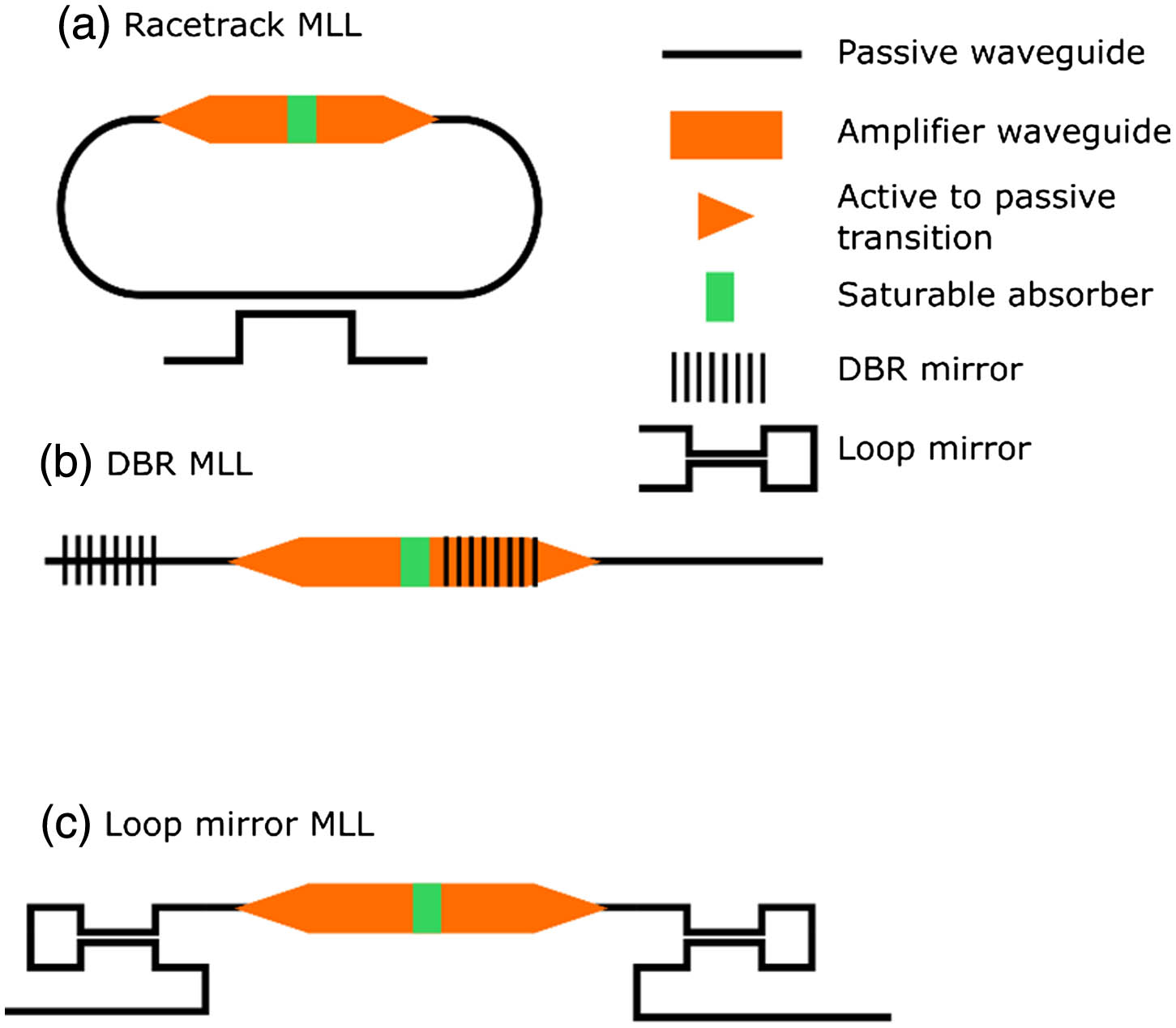
    Fig. 1. Schematic of the most common forms of fully integrated mode-locked laser cavity designs.
    Pulse width of a selection of mode-locked laser diodes from the literature.
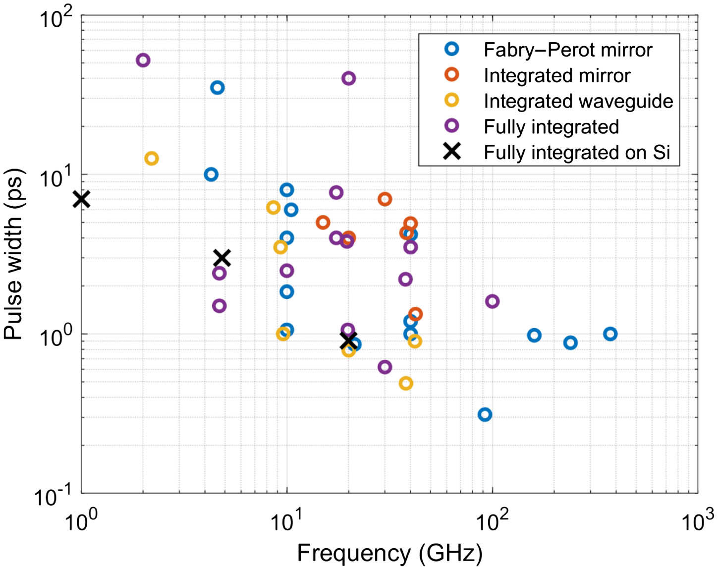
    Fig. 2. Pulse width of a selection of mode-locked laser diodes from the literature.
    Peak power of a selection of lasers from the literature, including this work. The colored lines represent approximate trends; purple is for fully integrated lasers, and blue is for Fabry–Perot lasers. The silicon lasers were not considered part of the trend.
    Fig. 3. Peak power of a selection of lasers from the literature, including this work. The colored lines represent approximate trends; purple is for fully integrated lasers, and blue is for Fabry–Perot lasers. The silicon lasers were not considered part of the trend.
    3 dB passively-mode locked RF linewidth of a selection of mode-locked lasers from the literature. The colored lines represent approximate trends; purple is for fully integrated lasers, and blue is for Fabry–Perot lasers. The silicon lasers and the two labeled outliers were not considered part of the trend.
    Fig. 4. 3 dB passively-mode locked RF linewidth of a selection of mode-locked lasers from the literature. The colored lines represent approximate trends; purple is for fully integrated lasers, and blue is for Fabry–Perot lasers. The silicon lasers and the two labeled outliers were not considered part of the trend.
    Schematic of the laser test device used in the experimental optimization.
    Fig. 5. Schematic of the laser test device used in the experimental optimization.
    Cross section of the heterogeneous amplifier waveguide. H+ denotes the hydrogen implanted section of the mesa. Current flows down only the central non-implanted p-type InP. The width of the underlying silicon waveguide controls the confinement factor. SCH, separate-confinement heterostructure; MQW, multi-quantum well.
    Fig. 6. Cross section of the heterogeneous amplifier waveguide. H+ denotes the hydrogen implanted section of the mesa. Current flows down only the central non-implanted p-type InP. The width of the underlying silicon waveguide controls the confinement factor. SCH, separate-confinement heterostructure; MQW, multi-quantum well.
    Dimensions of the heterogeneous transition.
    Fig. 7. Dimensions of the heterogeneous transition.
    Plan view schematics of the n-type transitions, showing (a) the n-type taper and (b) the n-type angle. In both cases, the p-type transition is the 30 μm three-section taper.
    Fig. 8. Plan view schematics of the n-type transitions, showing (a) the n-type taper and (b) the n-type angle. In both cases, the p-type transition is the 30 μm three-section taper.
    Pulse width versus the absorber length, plotted as a percentage fraction of the gain section length. In this case, with a 2-mm-long gain section, the absorber sections were 50, 100, 150, and 200 μm.
    Fig. 9. Pulse width versus the absorber length, plotted as a percentage fraction of the gain section length. In this case, with a 2-mm-long gain section, the absorber sections were 50, 100, 150, and 200 μm.
    Impact on the pulse width of increasing confinement factor in the pumped current channel region of the quantum well. The quantum well confinement factor is plotted versus waveguide width in the inset.
    Fig. 10. Impact on the pulse width of increasing confinement factor in the pumped current channel region of the quantum well. The quantum well confinement factor is plotted versus waveguide width in the inset.
    Pulse width versus the quantum well compressive strain in the active region.
    Fig. 11. Pulse width versus the quantum well compressive strain in the active region.
    Size comparison of the circular-bend loop mirror and the two spline-curve loop mirrors.
    Fig. 12. Size comparison of the circular-bend loop mirror and the two spline-curve loop mirrors.
    LI characteristic of the three loop mirror split lasers, with the absorbers forward biased at the same current density as the gain sections.
    Fig. 13. LI characteristic of the three loop mirror split lasers, with the absorbers forward biased at the same current density as the gain sections.
    Simulated bend loss for the narrow 400-nm-wide and 500-nm-tall waveguide used for the directional coupler and loop mirror.
    Fig. 14. Simulated bend loss for the narrow 400-nm-wide and 500-nm-tall waveguide used for the directional coupler and loop mirror.
    Pulse width versus loop mirror minimum bend radius. The 25-μm-bend mirror has fully circular bends. The 5-μm- and 3-μm-bend mirrors have the spline curve. The 3-μm-bend mirror resulted in the shortest pulse from the entire study, at 900 fs. The “Best integrated InP” result refers to Ref. [52], and the “Best of all Si” result refers to [34].
    Fig. 15. Pulse width versus loop mirror minimum bend radius. The 25-μm-bend mirror has fully circular bends. The 5-μm- and 3-μm-bend mirrors have the spline curve. The 3-μm-bend mirror resulted in the shortest pulse from the entire study, at 900 fs. The “Best integrated InP” result refers to Ref. [52], and the “Best of all Si” result refers to [34].
    Autocorrelation trace (blue) and sech2 fit (red dashes) of the 3-μm-bend spline-curve-mirror laser producing a 900 fs pulse.
    Fig. 16. Autocorrelation trace (blue) and sech2 fit (red dashes) of the 3-μm-bend spline-curve-mirror laser producing a 900 fs pulse.
    RF tone from the 5-μm-bend spline curve mirror laser (red) and Voigt fit (blue), showing 1.1 kHz linewidth.
    Fig. 17. RF tone from the 5-μm-bend spline curve mirror laser (red) and Voigt fit (blue), showing 1.1 kHz linewidth.
    Close-in view of the RF tone from the 5-μm-bend spline curve mirror laser showing the 1.1 kHz, 3 dB linewidth, along with some spurs at 2 and 4 kHz offset.
    Fig. 18. Close-in view of the RF tone from the 5-μm-bend spline curve mirror laser showing the 1.1 kHz, 3 dB linewidth, along with some spurs at 2 and 4 kHz offset.
    Optical spectrum from the 3-μm-bend spline curve mirror laser while it was producing the 900 fs pulse. The 3-dB bandwidth of the comb is 2.96 nm.
    Fig. 19. Optical spectrum from the 3-μm-bend spline curve mirror laser while it was producing the 900 fs pulse. The 3-dB bandwidth of the comb is 2.96 nm.
    LI characteristic from the 3-μm-bend laser under −4.5 V reverse bias. The shortest pulse came at 89 mA bias current, when the CW power was 1.83 mW. This corresponds to 98 mW peak power.
    Fig. 20. LI characteristic from the 3-μm-bend laser under 4.5  V reverse bias. The shortest pulse came at 89 mA bias current, when the CW power was 1.83 mW. This corresponds to 98 mW peak power.
    P Transition StyleN Transition StylePulse Width (ps)
    15 μm basicTaper3.45
    15 μm basicAngle2.70
    30 μm conformalTaper2.54
    30 μm conformalAngle2.34
    Table 1. Effect of Transition Design on Pulse Width
    Michael L. Davenport, Songtao Liu, John E. Bowers. Integrated heterogeneous silicon/III–V mode-locked lasers[J]. Photonics Research, 2018, 6(5): 468
    Download Citation