
Hao-Hao Ma, Xian-Bin Zhang, Xu-Yan Wei, Jia-Meng Cao. Theoretical study on Schottky regulation of WSe2/graphene heterostructure doped with nonmetallic elements [J]. Acta Physica Sinica, 2020, 69(11): 117101-1
- Acta Physica Sinica
- Vol. 69, Issue 11, 117101-1 (2020)
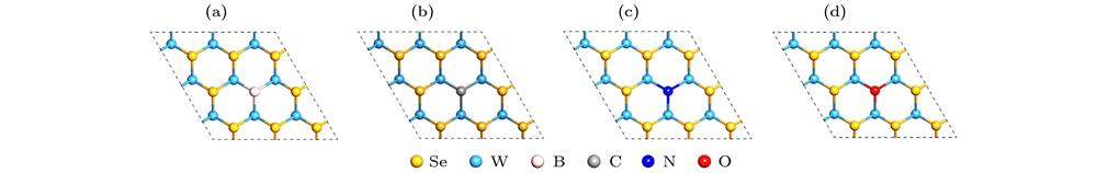
Fig. 1. Top views of monolayer WSe2 doping: (a) Top view of single layer WSe2 3 × 3 × 1 supercell boron doped; (b) top view of single layer WSe2 3 × 3 × 1 supercell carbon doped; (c) top view of single layer WSe2 3 × 3 × 1 supercell nitrogen doped; (d) top view of single layer WSe2 3 × 3 × 1 supercell oxygen doped.
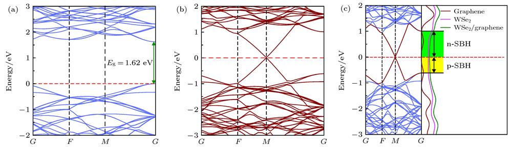
Fig. 2. Energy band structures of (a) monolayer WSe2, (b) grapheme, and (c) WSe2/graphene heterostructure. The n-type (p-type) SBH are indicated between the Fermi level and the conduction band minimum (the valence band maximum) of the WSe2 layer. The Fermi level is set to zero and marked by red dotted lines.
Fig. 3. Three-dimensional charge density difference plots of WSe2/graphene heterostructure: (a) Side view; (b) top view.
Fig. 4. Calculated total density of states and the corresponding partial density of states of WSe2/graphene heterostructure.
Fig. 5. Band structures: (a) W9Se17O1; (b) W9Se17N1; (c) W9Se17C1; (d) W9Se17B1.
Fig. 6. Band structures: (a) W9Se17O1/graphene; (b) W9Se17N1/graphen; (c) W9Se17C1/graphen; (d) W9Se17B1/graphen.
|
Table 1.
Lattice mismatch rate, formation energy, cohesive energy, and lattice mismatch energy parameters of WSe2/graphene heterojunction doped with different nonmetallic elements.
不同非金属元素掺杂WSe2/graphene异质结的晶格失配率、形成能、结合能、晶格失配能参数

Set citation alerts for the article
Please enter your email address
© Copyright 2018-2021 | Chinese Laser Press. All Rights Reserved 沪ICP备15018463号-20