
Guang-Hui Hao, Pan-Yang Han, Xing-Hui Li, Ze-Peng Li, Yu-Juan Gao. The electron emission characteristics of GaAs photocathode with vacuum-channel structure [J]. Acta Physica Sinica, 2020, 69(10): 108501-1
- Acta Physica Sinica
- Vol. 69, Issue 10, 108501-1 (2020)
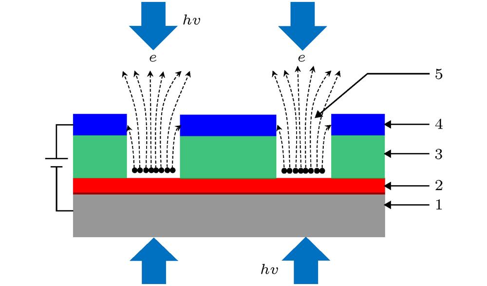
Fig. 1. Working principle of photocathode with vacuum channel. Symbol 1, 2, 3, 4 and 5 are negative electrode, photocathode material, insulation, grid electrode and vacuum channel, respectively.
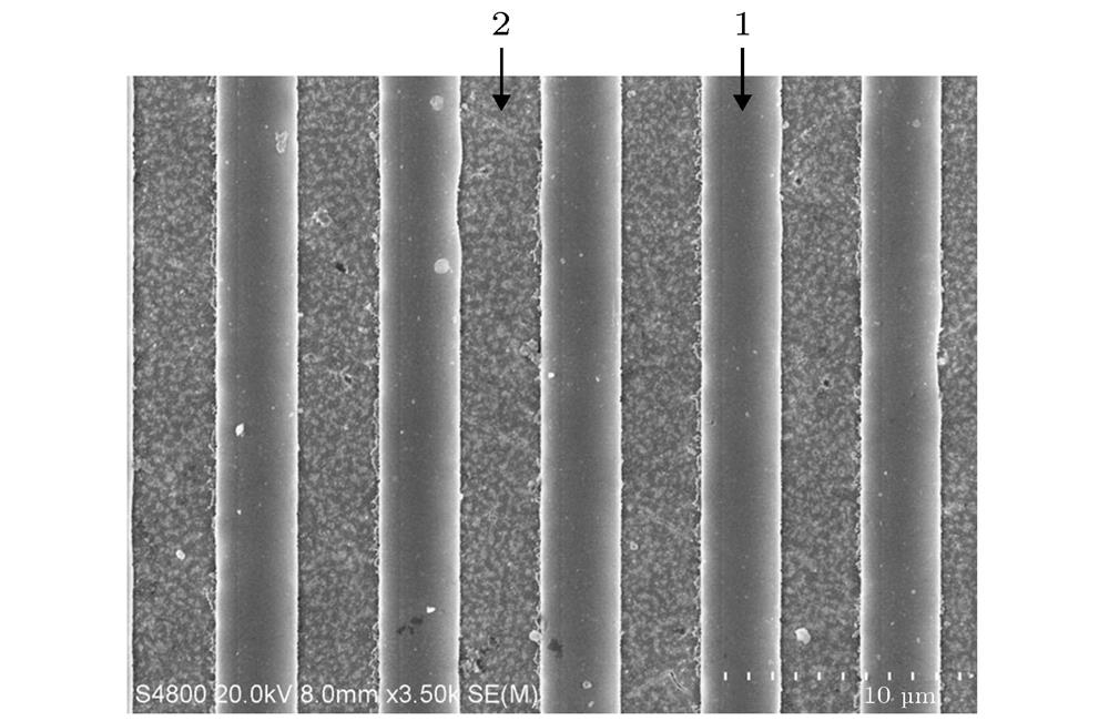
Fig. 2. Surface microtopography of vacuum channel structure. Symbol 1 and 2 are photocathode material grid electrode, respectively.
Fig. 3. DC emission characteristics of photocathode module with different laser bean power.
Fig. 4. DC emission characteristics of photocathode module with different temperature.
Fig. 5. The lifetime test curve of photocathode module.
Fig. 6. Simulation model of photocathode module with rectangular vacuum channel. Symbol 1, 2, 3 and 4 are photocathode material, insulation, grid electrode and positive electrode, respectively.
Fig. 7. Electronic distribution of lateral interface of photocathode module electron beam with rectangular vacuum channel.
Fig. 8. Simulation of electronic emission characteristics of photocathode module with circular vacuum channel: (a) Structure model; (b) electronic distribution of lateral interface. Symbol 1, 2 and 3 are photocathode material, insulation, and grid electrode, respectively.

Set citation alerts for the article
Please enter your email address
© Copyright 2018-2021 | Chinese Laser Press. All Rights Reserved 沪ICP备15018463号-20