
Guang-Zheng Zhou, Ying Li, Tian Lan, Jing-Jing Dai, Cong-Cong Wang, Zhi-Yong Wang. Design and simulation of integration of vertical cavity surface emitting lasers and heterojunction bipolar transistor [J]. Acta Physica Sinica, 2019, 68(20): 204203-1
- Acta Physica Sinica
- Vol. 68, Issue 20, 204203-1 (2019)
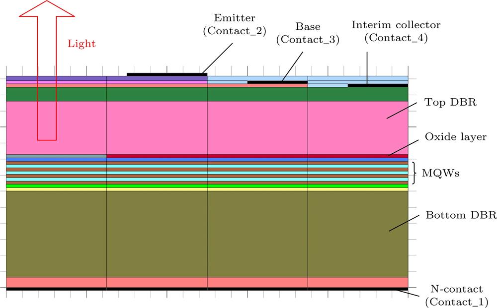
Fig. 1. Schematic diagram of integration of VCSELs and HBT.VCSELs与HBT集成结构示意图
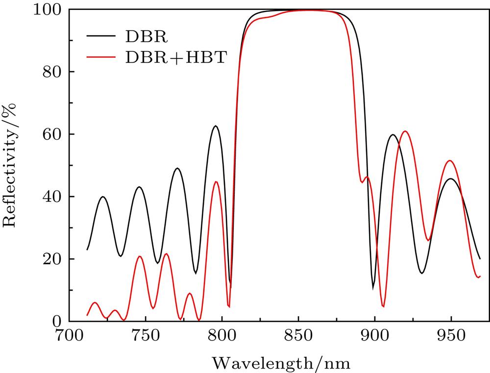
Fig. 2. Reflectivity of different DBRs.不同结构DBR反射率
Fig. 3. Band diagram of integrated structure at equilibrium.平衡态时集成结构的能带
Fig. 4. Integrated structure when HBT is in an amplified state: (a) Band diagram; (b) current distribution.HBT处于放大状态时的(a)能带图, (b)集成结构内部电流分布
Fig. 5. Integrated structure when both HBT and VCSELs were conducted: (a) Band diagram; (b) current distribution.HBT和VCSEL同时导通时的集成结构 (a)能带图; (b)内部电流分布
Fig. 6. Relations of interim collector currentwith voltage of interim collector.过渡集电极和N型电极电流随过渡集电极电压的变化
Fig. 7. I 1 varying with V 1 at different base currents.
不同基极电流下N型电极电流随电压的变化
Fig. 8. Output power varying with V 1 at different base currents.
不同基极电流下输出光功率随N型电极电压的变化
Fig. 9. (a) Temperature distribution of the device at a 10 μA base current; (b) temperature in active region and output power varying with the base current (V 1 = –6 V).
(a)基极电流为10 μA时器件内部温度分布; (b)有源区温度和输出光功率随基极电流的变化(V 1 = –6 V)
Fig. 10. The ac power gain of integration structure.集成结构的交流光增益

Set citation alerts for the article
Please enter your email address
© Copyright 2018-2021 | Chinese Laser Press. All Rights Reserved 沪ICP备15018463号-20