Abstract
The finite-difference time-domain method was employed to calculate light extraction efficiency of thin-film flip-chip InGaN/GaN quantum well light-emitting diodes (LEDs) with TiO2 microsphere arrays. The extraction efficiency for LEDs with microsphere arrays was investigated by focusing on the effect of the packing density, packing configuration, and diameter-to-period ratio. The comparison studies revealed the importance of having a hexagonal and close-packed monolayer microsphere array configuration for achieving optimum extraction efficiency, which translated into a 3.6-fold enhancement in light extraction compared to that for a planar LED. This improvement is attributed to the reduced Fresnel reflection and enlarged light escape cone. The engineering of the far-field radiation patterns was also demonstrated by tuning the packing density and packing configuration of the microsphere arrays.1. INTRODUCTION
Significant advances have been achieved in the field of III-nitride semiconductor materials and devices. The applications of these III-nitride technologies have impacted solid-state lighting [1–6], thermoelectricity [7,8], lasers [9,10], and solar energy conversion [11]. The application of III-nitride-based light-emitting diodes (LEDs) has been implemented for solid-state lighting, specifically as blue emitters in white LED configurations. The key advances in III-nitride LEDs have also been recognized for the 2014 Nobel Prize in physics [12]. The advances in the fields of nitride-based LEDs were driven strongly by innovations in material epitaxy [13] and nanostructure active region engineering [14–17] for improved internal quantum efficiency, solutions for addressing the efficiency-droop issue [18–21], and approaches to achieving improved extraction [22–25] in LEDs. The optimizations of both internal and extraction efficiencies in LEDs are instrumental in achieving optimized external quantum efficiency for LED emitters.
Approaches that address the light extraction limitation in a cost-effective and scalable manner are instrumental for addressing the extraction limitation in LEDs for wide implementation. The flip-chip technology was developed to avoid the absorption of semitransparent metal of conventional top emitting devices, resulting in a 1.6-fold improvement over that of the conventional top-emitting LED [22]. Other methods such as surface roughening [26], embedded photonic crystals [27–29], self-assembled lithography p-GaN patterning [30], GaN microdomes [31,32], micropillars [33], nanopyramids [34], and shape design [35] were employed to improve light extraction efficiency as well. Sapphire microlenses [36,37], oblique mesa sidewalls [38], nanowires [39], and the graded refractive index [40] were also employed to enhance the extraction efficiency. To further enhance the light extraction efficiency, a thin-film flip-chip (TFFC) LED structure can provide surface brightness and flux output advantages over conventional flip-chip LEDs [23,24], and this technology is widely used in industry today. Approaches to improve the extraction efficiency in TFFC LEDs have been pursued by using surface roughening and photonic crystal. Though the surface roughening approach results in a 2- to 3-fold enhancement in light extraction efficiency, the photochemical etching process led to a nonuniform surface and provided no control over the far-field radiation pattern of the extracted light. The electrical properties of LEDs could also be degraded via the use of photochemical etching [41–43]. The photonic crystal method results in state-of-the-art results for TFFC LEDs, with a 2.3-fold enhancement in light extraction efficiency [44]; however, this approach requires a relatively expensive e-beam lithography fabrication step.
Recently, we have demonstrated the use of colloidal-based microsphere and microlens arrays deposited via a scalable rapid convective deposition (RCD) process, resulting in improved light extraction efficiency for GaN-based LEDs [45–52] with a cost-effective approach. By using a binary deposition and heat treatment process, microlens arrays can be formed [48]. The use of these colloidal microsphere/microlens arrays has also been implemented in organic LEDs, resulting in a 3-fold enhancement in power conversion efficiency [48].
Sign up for Photonics Research TOC. Get the latest issue of Photonics Research delivered right to you!Sign up now
In this work, we present an investigation on the effect of packing configuration and packing density of microsphere arrays on top of GaN-based TFFC LEDs. By optimizing the deposition parameter in the RCD process, the ability to tune the packing density (submonolayer, monolayer, or multilayer) and packing configuration (square or hexagonal lattice) of the microsphere arrays can be achieved on top of the GaN surface, which was shown in our prior work [47]. The present study focuses on identification of the optimum configuration and density required to achieve optimized extraction in LED devices. Our analysis was carried out by using numerical simulation based on the finite-difference time-domain (FDTD) method for analyzing the light extraction efficiency of III-nitride TFFC LEDs employing refractive-index-matched anatase microsphere arrays with various packing density and packing geometries. The selection of for the microspheres in our previous works [45–48] had been primarily motivated from the ease in obtaining the silica-based spheres with a wide range of dimensions commercially. Recently, our FDTD calculation showed that the best material for the microsphere arrays for GaN LED applications is refractive-index-matched anatase microsphere arrays [51], which have also recently been implemented experimentally [52].
2. FDTD ANALYSIS OF LIGHT EXTRACTION EFFICIENCY
In this study, we employed the microsphere arrays on top of a TFFC GaN LED device structure, as shown in Fig. 1. Note that the goals of the present study will be limited to determining the optimum packing density and packing configuration, as well as the corresponding far-field radiation patterns for the LEDs employing microsphere arrays. The optimization of the extraction efficiency will require the optimization of the resonant condition in TFFC thickness [40]. In this structure, the InGaN/GaN quantum well (QW) was sandwiched between p-GaN and n-GaN. The thickness of the TFFC studied follows the structure presented in Ref. [53]. A metallic mirror was attached to the bottom of the p-GaN to reflect the light back to the LED device, and finally the light was extracted from the top of the LED devices. Microsphere arrays with various ratios of diameter to lattice period () and packing shape were deposited on top of the LEDs; they were obtained by tuning the deposition speed [45–47]. Our prior works had demonstrated that the deposition of micro/nanosphere arrays with diameters ranging from 100 nm up to 1 μm performed consistently on the devices [45–50,52]. The use of a 500 nm diameter sphere was based on practical consideration of the ease of sphere synthesis and the highly uniform deposition of these microsphere arrays on LEDs [51]. Our prior works have also shown that the 500 nm microsphere diameter falls within the optimum diameter range for achieving maximum light extraction efficiency for emitting III-nitride LEDs [52].
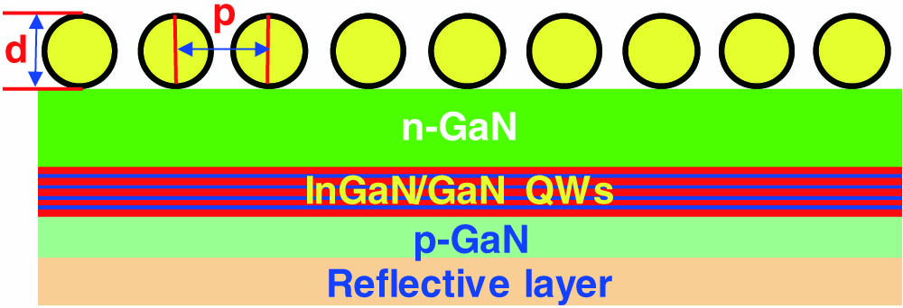
Figure 1.Cross sectional schematic of the simulated LED device structure employing microsphere arrays.
In our simulation, the 3D LED devices were formed with appropriate boundary conditions. The real LED device is in the lateral direction. The 3D FDTD method requires a large amount of memory and computing time. For the purpose of computational efficiency, in this calculation, we set the simulation domain to be with perfectly matched layer boundary conditions applied to the lateral boundaries to avoid unnecessary reflection of light at the boundaries, and the perfect electrical conductor (PEC) boundary conditions were implemented to the bottom of the LED to represent the metallic mirror. The grid size was set to be 10 nm to ensure the accuracy of the results. The time step was determined by the grid size and Courant condition. The simulation time was set to be large enough to ensure stabilized field output.
Seven dipoles were chosen as the light source within the QW region and positioned in the center region of the QW within one period of the spheres. The emission wavelength used in this calculation was set to . Note that our work focuses on clarifying the optimum packing density and packing configuration of the microsphere arrays for light extraction efficiency in visible III-nitride LEDs, and the choice of the wavelength will not affect the conclusion derived from this study.
In our computation, two monitors were used to measure the power radiating from the dipoles and the power extracted out of the microsphere arrays, respectively. A hidden monitor surrounding the dipole was used to measure the power radiating from the dipole. Another monitor was placed 300 nm above the LED device and one grid point below the domain maximum to measure the extracted power.
The far-field electric field [] was obtained from the near-field electric field [] by Fourier transformation. The plane wave relation was used to calculate the magnetic field in the far-field region. The total output power extracted from the LED device () was obtained by integrating the power density in the far-field region over the whole solid angle. Last, the light extraction efficiency was calculated as the ratio of the optical output power extracted from the LED device to the total power generated in the InGaN/GaN multiple quantum wells (MQWs) active region.
3. RCD OF MICROSPHERE ARRAYS WITH VARYING PACKING DENSITY AND GEOMETRY
The fabrication of microsphere arrays on top of LEDs can be performed by the rapid RCD method. RCD enables controlled deposition for self-assembled microsphere arrays with submonolayer, monolayer, and multilayer packing densities via a roll-to-roll printing method. RCD is a self-assembly process for depositing the negatively charged particles under the capillary force, and the deposition velocity () will dictate the packing densities and configurations of the microsphere arrays, which have been articulated in our prior works [47,54]. The critical deposition velocity () for achieving monolayer packing density was shown in our earlier work [47,54] as identical to the film growth rate, as follows: where depends on the evaporation rate that is determined by the temperature and humidity, which should remain constant. denotes the height of the thin film, which is equal to the diameter of the microsphere for the monolayer, and the parameter ε represents the porosity of the colloidal crystal. In other words, is the packing fraction of the colloidal crystal, which is 0.605 for hexagonal close-packed sphere arrays and 0.52 for square close-packed spheres arrays. The parameter signifies the constant volume fraction of the microsphere suspension. Note that the monolayer is obtained when the substrate withdrawal speed is equal to the film growth rate, and the submonolayer is obtained when the substrate withdrawal speed is higher than the film growth rate. Otherwise, the multilayer is obtained when the substrate withdrawal speed is lower than the crystal growth rate. By varying the deposition speed (), microsphere arrays with different packing densities and packing geometries—hexagonal close-packed monolayer [Fig. 2(a)], square close-packed monolayer [Fig. 2(b)], submonolayer [Fig. 2(c)], and multilayer [Fig. 2(d)]—can be obtained [47]. The studies on the effect of the packing density will be carried out in Section 4, and the comparison of the light extraction efficiencies in LEDs with different packing geometries (hexagonal versus square lattice) will be presented in Section 5.

Figure 2.Schematic of the microsphere LEDs (a) with hexagonal close-packed sphere array, (b) with square close-packed sphere array, (c) with submonolayer sphere array, and (d) with multilayer microsphere arrays.
4. EFFECT OF PACKING DENSITY ON THE LIGHT EXTRACTION EFFICIENCY OF MICROSPHERE ARRAY LEDS
In order to investigate the effect of the packing density of the microsphere arrays on the light extraction efficiency of the LED, we calculated the light extraction efficiency of LEDs deposited with submonolayer, monolayer, and multilayer microsphere () arrays with a hexagonal packing geometry. Figures 3(a)–3(c) show the light extraction efficiency enhancement of microsphere array LEDs with various values. Here, is defined as the ratio of the diameter to the lattice period. Note that the hexagonal close-packed monolayer microsphere array has an of 1. Otherwise, the microsphere array becomes submonolayer when is smaller than 1, and it becomes multilayer when the is larger than 1. The light extraction efficiency of GaN LEDs with microsphere arrays and a flat planar LED were calculated for microsphere arrays with various values. The ratios of the light extraction efficiencies of the LEDs with microsphere arrays to that of the planar LED are shown in Fig. 3(a). The far-field radiation patterns of these LEDs for an azimuthal direction of were plotted in Fig. 3(b), and the corresponding angle-dependent (in the direction) power density comparison data for microsphere LEDs were shown in Fig. 3(c).
Figure 3.(a) Ratio of light extraction efficiency of microsphere LEDs with various sphere packing densities to that of the planar LED, (b) comparison of far-field intensity of microsphere LEDs with various packing densities at , (c) angle-dependent power distribution.
As the increases from the submonolayer condition () to a close-packed configuration (), the light extraction efficiency increases, resulting in an -fold enhancement for the case of monolayer array structures. As the is larger than for the monolayer condition, the enhancement observed started to decrease for the multilayer structures. This finding is important in confirming the significance of close-packed monolayer array structures. Previously, there was no clear quantitative work that demonstrated the importance and value of justifying the approaches that achieve monolayer close-packed microsphere arrays. However this finding clearly shows that the monolayer and close-packed configuration is essential for achieving optimum light extraction. Any increase in multilayer packing density was shown to reduce the extraction efficiency despite the increase in scattering centers.
The comparison of the far-field radiation patterns for the planar LED, LED with submonolayer sphere array, LED with monolayer sphere array, and LED with multilayer sphere array is presented in Fig. 4. The far-field radiation pattern for the planar LED exhibits Lambertian radiation patterns with only an angle-dependent and symmetrically azimuthal distribution. The far-field intensity of the planar LED is much weaker in all angular direction compared to those of the LEDs with microsphere arrays due to the small light escape cone, and only a small amount of light can be extracted from the LED device. The inner and outer radiation rings are attributed to the direct emission from the InGaN QWs and reflected emission by the PEC reflectors, respectively. The LEDs with microsphere arrays exhibit both angular and azimuthal dependence, as shown in Figs. 4(b)–4(d). The significantly higher intensities are observed in the far-field radiation patterns of the microsphere array LEDs for both the normal and large angular distribution, and in turn result in improved light extraction efficiency for these LEDs. The far-field intensity of LEDs with microsphere arrays exhibits hexagonal symmetry due to hexagonal packed nature of the sphere arrays. However, the light distributions along the angular direction and azimuthal direction for LEDs with submonolayer sphere arrays, monolayer arrays, and multilayer arrays are very different. For the LED with a submonolayer microsphere array, most of the light is extracted in the normal direction, while only a small amount of light is extracted in the larger angular direction. For the case of the LED with a monolayer sphere array, the light is spread over a larger surface, and it can be extracted in relatively larger angular range, which results in improved light extraction efficiency. The same phenomenon was observed for the LED with a multilayer sphere array, but the light intensity is much lower than that of the LED with a monolayer sphere array, which led to a relatively lower light extraction ratio compared to the monolayer case. Note that the comparison of light extraction efficiency between microsphere array LEDs and the planar LED was carried out by taking the total output power integrated over the whole solid angle.
Figure 4.Contour plots of far-field intensity of microsphere LED (b) with a submonolayer sphere array (), (c) with a monolayer sphere array (), and (d) with a multilayer sphere array (). The contour plot of the far-field radiation pattern of (a) the planar LED is included for reference.
In order to provide a quantitative comparison, the far-field radiation patterns of these LEDs were plotted for a particular azimuthal direction of [see Fig. 3(b)]. The comparison of angle-dependent power density for the planar LED and LEDs with microsphere arrays was also plotted. The microsphere array LEDs exhibit a significant increase in the intensity of the far-field radiation pattern for all angular distributions, as shown in Fig. 3(c). Furthermore, the contribution of a larger angular component in the far-field radiation pattern is significantly increased for the microsphere LED with a hexagonal close-packed monolayer geometry [Fig. 3(c)], which results in an increase of the total power extracted from this microsphere array LED. Note that the enhancement of the TFFC LED with a monolayer microsphere array is greater than that of conventional top-emitting LED devices with monolayer microsphere arrays [51]. This is due to the different boundary conditions we used for the calculation. In this calculation, the PEC boundary condition was used to reflect the light back to the LED devices, and finally the light has a better chance of being extracted with the help of microsphere arrays.
5. EFFECT OF PACKING GEOMETRY ON FAR-FIELD RADIATION PATTERNS OF MICROSPHERE ARRAY LEDS
As presented in Section 4, the microsphere array with monolayer packing density has been demonstrated as the best option for maximizing the light extraction efficiency of the LED. In addition to the packing density, the packing geometry of the microsphere arrays also plays an important role in optimizing the light extraction efficiency and far-field radiation patterns of the LEDs. Therefore, different types of packing geometries (hexagonal and square close-packed lattice) of the monolayer microsphere array were investigated to compare their corresponding far-field radiation patterns and extraction characteristics. Note that the square or hexagonal close-packed monolayer can be obtained by adjusting the proper substrate deposition speed () to be equal to the crystal growth speed under the condition that the packing fraction equals to 0.52, as elaborated previously [47].
Figures 5(a) and 5(b) show the far-field light radiation patterns of the LEDs with hexagonal [Fig. 5(c)] and square [Fig. 5(d)] close-packed monolayer microsphere arrays, respectively. These two different packing geometries exhibit similar far-field radiation patterns, implying enhancement of the light intensity in the normal direction and a larger angular distribution compared to those of the planar LED. However, the far-field radiation patterns of hexagonal and square close-packed structures exhibit different symmetries. The far-field radiation pattern presents a hexagonal pattern for the LED with a hexagonal close-packed microsphere structure but a square pattern for the LED with a square close-packed microsphere array. The differences in symmetry are attributed to the different microsphere arrangements, which have a significant effect on the far-field radiation pattern due to the scattering effect of light.
Figure 5.Far-field radiation patterns of LEDs with (a) hexagonal close-packed anatase- sphere array and (b) square close-packed anatase- sphere array; (c) schematic of hexagonal close-packed sphere array and (d) schematic of square close-packed sphere array.
In order to further investigate the effect of spheres on the light distribution and light extraction efficiency, we also plotted the far-field radiation patterns of LEDs with various numbers of spheres for both hexagonal packed arrays and square packed arrays, as shown in Fig. 6. Note that all the spheres were packed in the center region of the devices. The far-field radiation pattern of the planar LED was also plotted for comparison. The comparison study here is to provide an observation on how the far-field radiation patterns and light extraction efficiencies in microsphere array LEDs are directly affected by an increased escape cone, which can be shown by the significantly enhanced light intensity around the sphere region as the number of spheres in the arrays increases.
Figure 6.Contour plots of the far-field intensity of microsphere LEDs with microsphere arrays: (a) flat LED, (b) hexagonal close-packed sphere array with 7 spheres, (c) hexagonal close-packed sphere array with 19 spheres, (d) hexagonal close-packed sphere array with 37 spheres, () one sphere in the center of the device, () square close-packed sphere array with 9 spheres, () square close-packed sphere array with 25 spheres, () square close-packed sphere array with 36 spheres. The corresponding schematics of the sphere arrays are shown in the top and bottom rows.
Figure 6(a) shows that the far-field radiation pattern of the planar LED has the perfect circular symmetry. However, as shown in Fig. 6(), the light extraction efficiency is enhanced at the center region when only one sphere is placed on top of the center region of the device. For the LEDs with hexagonal close-packed sphere arrays, the light intensity is significantly enhanced around the sphere region, as shown in Figs. 6(b) to 6(d). Similar light intensity enhancement is also demonstrated for the LEDs with square close-packed sphere arrays, as can be seen in Figs. 6() to 6(). Note that the enhancement of the LED always occurs in the region covered with the microsphere array. This further proves that the microsphere arrays not only reduce the Fresnel reflection but also scatter the light in a larger angular direction to increase the light escape cone, which results in enhanced light extraction efficiency of the LED. The quantitative comparisons of the angle-dependent (in the direction) power density comparison data for microsphere LEDs [Figs. 3(c) and 4(a)–4(d)] also exhibited significant enhancement in the large direction, which strongly indicated an increase in the effective escape cone in the microsphere array LEDs.
Slight enhancement in light extraction efficiency is observed for the hexagonal close-packed configuration in comparison to that obtained for the square close-packed array configuration, as shown in Fig. 7. This finding is consistent with the larger scattering center across the 2D lateral distribution from the higher packing density enabled by hexagonal lattice arrays, which cause improved extraction efficiency. It is important to note that the self-assembled microsphere arrays formed by the colloidal deposition method result in many domains with highly ordered regions in the range of . The defect in the colloidal crystal results in domains with a poly-crystalline-like structure, which in turn may result in the averaging effect on the directionality studies in the analysis for large area devices. The extraction efficiency in microsphere array LEDs is minimally affected by the locally ordered domains, which has been demonstrated in numerous experimental results [45–50,52].
Figure 7.Ratio of the extraction efficiency for microsphere array LEDs with both hexagonal and square close-packed monolayer configurations with a varying number of spheres, similar to the ones presented in Fig. 6. The results are normalized to the extraction of planar LEDs.
6. CONCLUSION
The FDTD method was employed to calculate the light extraction efficiency of TFFC LEDs with -based microsphere arrays. Specifically, the light extraction efficiency of microsphere array LEDs with different packing densities (submonolayer, monolayer, and multilayer) and different packing geometries (square and hexagonal close-packed geometries) are compared. Our finding indicates that the optimized packing density and packing geometry of the microsphere arrays for the LEDs is the hexagonal close-packed monolayer sphere array. By optimizing the lattice structure of microsphere arrays, the light extraction efficiency of microsphere LEDs is expected to have 3.6-fold enhancement compared to that of a planar LED. The far-field pattern engineering can also be achieved by selecting hexagonal and square lattice configurations, and the use of hexagonal patterns appears to provide a slight increase in the light extraction efficiency in comparison to that from a square lattice.
Sign up for Photonics Research TOC. Get the latest issue of Photonics Research delivered right to you!Sign up now
ACKNOWLEDGMENT
Acknowledgment. The work was supported in part by the U.S. Department of Energy (Grant No. NE TL, DE-PS26-08NT00290), in part by the National Science Foundation (ECCS-1408051, CBET-1120399), and in part by the Daniel E. ’39 and Patricia M. Smith Endowed Chair Professorship Fund. The authors also would like to acknowledge useful discussions with Wei Sun and Chee-Keong Tan, both from Lehigh University.
References
[1] M. H. Crawford. LEDs for solid-state lighting: performance challenges and recent advances. IEEE J. Sel. Top. Quantum Electron., 15, 1028-1040(2009).
[2] N. Tansu, H. P. Zhao, G. Y. Liu, X. H. Li, J. Zhang, H. Tong, Y. K. Ee. III-nitride photonics. IEEE Photon. J., 2, 241-248(2010).
[3] J. Y. Tsao, M. H. Crawford, M. E. Coltrin, A. J. Fischer, D. D. Koleske, G. S. Subramania, G. T. Wang, J. J. Wierer, R. F. Karlicek. Toward smart and ultra-efficient solid-state lighting. Adv. Opt. Mater., 2, 809-836(2014).
[4] H. Zhao, J. Zhang, G. Liu, N. Tansu. Surface plasmon dispersion engineering via double-metallic Au/Ag layers for III-nitride based light emitting diodes. Appl. Phys. Lett., 98, 151115(2011).
[5] I. H. Brown, P. Blood, P. M. Smowton, J. D. Thomson, S. M. Olaizola, A. M. Fox, P. J. Parbrook, W. W. Chow. Time evolution of the screening of piezoelectric fields in InGaN quantum wells. IEEE J. Quantum Electron., 42, 1202-1208(2006).
[6] J. H. Ryou, P. D. Yoder, J. Liu, Z. Lochner, H. Kim, S. Choi, H. J. Kim, R. D. Dupuis. Control of quantum-confined stark effect in InGaN-based quantum wells. IEEE J. Sel. Top. Quantum Electron., 15, 1080-1091(2009).
[7] X. Li, S. Kim, E. E. Reuter, S. G. Bishop, J. J. Coleman. The incorporation of arsenic in GaN by metalorganic chemical vapor deposition. Appl. Phys. Lett., 72, 1990-1992(1998).
[8] B. N. Pantha, I. Feng, K. Aryal, J. Li, J. Y. Lin, H. X. Jiang. Erbium-doped AlInGaN alloys as high-temperature thermoelectric materials. Appl. Phys. Express, 4, 051001(2011).
[9] J. Zhang, H. Tong, G. Liu, J. A. Herbsommer, G. S. Huang, N. Tansu. Characterizations of Seebeck coefficients and thermoelectric figures of merit for AlInN alloys with various in-contents. J. Appl. Phys., 109, 053706(2011).
[10] M. Kneissl, D. W. Treat, M. Teepe, N. Miyashita, N. M. Johnson. Continuous-wave operation of ultraviolet InGaN/InAlGaN multiple-quantum-well laser diodes. Appl. Phys. Lett., 82, 2386-2388(2003).
[11] R. Dahal, B. Pantha, J. Li, J. Y. Lin, H. X. Jiang. InGaN/GaN multiple quantum well solar cells with long operating wavelengths. Appl. Phys. Lett., 94, 063505(2009).
[12] .
[13] Y. K. Ee, J. M. Biser, W. J. Cao, H. M. Chan, R. P. Vinci, N. Tansu. Metalorganic vapor phase epitaxy of III-nitride light-emitting diodes on nanopatterned AGOG sapphire substrate by abbreviated growth mode. IEEE J. Sel. Top. Quantum Electron., 15, 1066-1072(2009).
[14] H. Zhao, G. Y. Liu, J. Zhang, J. D. Poplawsky, V. Dierolf, N. Tansu. Approaches for high internal quantum efficiency green InGaN light-emitting diodes with large overlap quantum wells. Opt. Express, 19, A991-A1007(2011).
[15] R. A. Arif, Y. K. Ee, N. Tansu. Polarization engineering via staggered InGaN quantum wells for radiative efficiency enhancement of light emitting diodes. Appl. Phys. Lett., 91, 091110(2007).
[16] D. F. Feezell, J. S. Speck, S. P. DenBaars, S. Nakamura. Semipolar (2021) InGaN/GaN light-emitting diodes for high-efficiency solid-state lighting. J. Display Technol., 9, 190-198(2013).
[17] C. K. Tan, N. Tansu. Nanostructured lasers: electrons and holes get closer. Nat. Nanotechnol., 10, 107-109(2015).
[18] C. H. Wang, S. P. Chang, W. T. Chang, J. C. Li, Y. S. Lu, Z. Y. Li, H. C. Yang, H. C. Kuo, T. C. Lu, S. C. Wang. Efficiency droop alleviation in InGaN/GaN light-emitting diodes by graded-thickness multiple quantum wells. Appl. Phys. Lett., 97, 181101(2010).
[19] G. Y. Liu, J. Zhang, C. K. Tan, N. Tansu. Efficiency-droop suppression by using large-bandgap AlGaInN thin barrier layers in InGaN quantum-well light-emitting diodes. IEEE Photon. J., 5, 2201011(2013).
[20] J. Iveland, L. Martinelli, J. Peretti, J. S. Speck, C. Weisbuch. Direct measurement of Auger electrons emitted from a semiconductor light-emitting diode under electrical injection: identification of the dominant mechanism for efficiency droop. Phys. Rev. Lett., 110, 177406(2013).
[21] C. K. Tan, J. Zhang, X. H. Li, G. Y. Liu, B. O. Tayo, N. Tansu. First-principle electronic properties of dilute-As GaNAs alloy for visible light emitters. J. Display Technol., 9, 272-279(2013).
[22] J. J. Wierer, D. A. Steigerwald, M. R. Krames, J. J. O’Shea, M. J. Ludowise, G. Christenson, Y. C. Shen, C. Lowery, P. S. Martin, S. Subramanya, W. Götz, N. F. Gardner, R. S. Kern, S. A. Stockman. High-power AlGaInN flip-chip light-emitting diodes. Appl. Phys. Lett., 78, 3379-3381(2001).
[23] V. Haerle, B. Hahn, S. Kaiser, A. Weimar, S. Bader, F. Eberhard, A. Plossl, D. Eisert. High brightness LEDs for general lighting applications using the new ThinGaN technology. Phys. Status Solidi A, 201, 2736-2739(2004).
[24] O. B. Shchekin, J. E. Epler, T. A. Trottier, T. Margalith, D. A. Steigerwald, M. O. Holcomb, P. S. Martin, M. R. Krames. High performance thin-film flip-chip InGaN-GaN light-emitting diodes. Appl. Phys. Lett., 89, 071109(2006).
[25] S. J. Chang, C. S. Chang, Y. K. Su, C. T. Lee, W. S. Chen, C. F. Shen, Y. P. Hsu, S. C. Shei, H. M. Lo. Nitride-based flip-chip ITO LEDs. IEEE Trans. Adv. Packag., 28, 273-277(2005).
[26] T. Fujii, Y. Gao, R. Sharma, E. L. Hu, S. P. DenBaars, S. Nakamura. Increase in the extraction efficiency of GaN-based light-emitting diodes via surface roughening. Appl. Phys. Lett., 84, 855-857(2004).
[27] J. Jewell, D. Simeonov, S.-C. Huang, Y.-L. Hu, S. Nakamura, J. Speck, C. Weisbuch. Double embedded photonic crystals for extraction of guided light in light-emitting diodes. Appl. Phys. Lett., 100, 171105(2012).
[28] E. Matioli, C. Weisbuch. Impact of photonic crystals on LED light extraction efficiency: approaches and limits to vertical structure designs. J. Phys. D, 43, 354005(2010).
[29] K. H. Li, K. Y. Zang, S. J. Chua, H. W. Choi. III-nitride light-emitting diode with embedded photonic crystals. Appl. Phys. Lett., 102, 181117(2013).
[30] S. Chhajed, W. Lee, J. Cho, E. F. Schubert, J. K. Kim. Strong light extraction enhancement in GaInN light-emitting diodes by using self-organized nanoscale patterning of p-type GaN. Appl. Phys. Lett., 98, 071102(2011).
[31] P. Zhao, H. Zhao. Analysis of light extraction efficiency enhancement for thin-film-flip-chip InGaN quantum wells light-emitting diodes with GaN micro-domes. Opt. Express, 20, A765-A776(2012).
[32] L. Han, T. A. Piedimonte, H. Zhao. Experimental exploration of the fabrication of GaN microdome arrays based on a self-assembled approach. Opt. Mater. Express, 3, 1093-1100(2013).
[33] M. Ma, J. Cho, E. F. Schubert, Y. Park, G. B. Kim, C. Sone. Strong light-extraction enhancement in GaInN light-emitting diodes patterned with TiO2 micro-pillars with tapered sidewalls. Appl. Phys. Lett., 101, 141105(2012).
[34] J. Q. Xi, H. Luo, A. J. Pasquale, J. K. Kim, E. F. Schubert. Enhanced light extraction in GaInN light-emitting diode with pyramid reflector. IEEE Photon. Technol. Lett., 18, 2347-2349(2006).
[35] B. Sun, L. X. Zhao, T. B. Wei, X. Y. Yi, Z. Q. Liu, G. H. Wang, J. M. Li. Shape designing for light extraction enhancement bulk-GaN light-emitting diodes. J Appl. Phys., 113, 243104(2013).
[36] Y. Sheng, C. Xia, Z. M. Simon Li, L. Cheng. Simulation of InGaN/GaN light-emitting diodes with patterned sapphire substrate. Opt. Quantum Electron., 45, 605-610(2013).
[37] J. W. Pan, P. J. Tsai, K. D. Chang, Y. Y. Chang. Light extraction efficiency analysis of GaN-based light-emitting diodes with nanopatterned sapphire substrates. Appl. Opt., 52, 1358-1367(2013).
[38] J. S. Lee, J. Lee, S. Kim, H. Jeon. Fabrication of reflective GaN mesa sidewalls for the application to high extraction efficiency LEDs. Phys. Stat. Sol. C, 4, 2625-2628(2007).
[39] Y. Qingyang, L. Kang, K. Fanmin, Z. Jia, L. Wei. Analysis on the light extraction efficiency of GaN-based nanowires light-emitting diodes. IEEE J. Quantum Electron., 49, 697-704(2013).
[40] J. Q. Xi, M. F. Schubert, J. K. Kim, E. F. Schubert, M. F. Chen, S. Y. Lin, W. Liu, J. A. Smart. Optical thin-film materials with low refractive index for broadband elimination of Fresnel reflection. Nat. Photonics, 1, 176-179(2007).
[41] C. C. Kao, H. C. Kuo, K. F. Yeh, J. T. Chu, W. L. Peng, H. W. Huang, T. C. Lu, S. C. Wang. Light-output enhancement of nano-roughened GaN laser lift-off light-emitting diodes formed by ICP dry etching. IEEE Photon. Technol. Lett., 19, 849-851(2007).
[42] C. Huh, K. S. Lee, E. J. Kang, S. J. Park. Improved light-output and electrical performance of InGaN-based, light-emitting diode by microroughening of the p-GaN surface. J Appl. Phys., 93, 9383-9385(2003).
[43] H. W. Huang, J. T. Chu, C. C. Kao, T. H. Hseuh, T. C. Lu, H. C. Kuo, S. C. Wang, C. C. Yu. Enhanced light output of an InGaN/GaN light emitting diode with a nano-roughened p-GaN surface. Nanotechnology, 16, 1844-1848(2005).
[44] J. J. Wierer, A. David, M. M. Megens. III-nitride photonic-crystal light-emitting diodes with high extraction efficiency. Nat. Photonics, 3, 163-169(2009).
[45] Y. K. Ee, P. Kumnorkaew, R. A. Arif, J. F. Gilchrist, N. Tansu. Enhancement of light extraction efficiency of InGaN quantum wells light emitting diodes using SiO2/polystyrene microlens arrays. Appl. Phys. Lett., 91, 221107(2007).
[46] Y. K. Ee, P. Kumnorkaew, R. A. Arif, H. Tong, H. Zhao, J. F. Gilchrist, N. Tansu. Optimization of light extraction efficiency of III-nitride LEDs with self-assembled colloidal-based microlenses. IEEE J. Sel. Top. Quantum Electron., 15, 1218-1225(2009).
[47] P. Kumnorkaew, Y. K. Ee, N. Tansu, J. F. Gilchrist. Investigation of the deposition of microsphere monolayers for fabrication of microlens arrays. Langmuir, 24, 12150-12157(2008).
[48] X. H. Li, R. Song, Y. K. Ee, P. Kumnorkaew, J. F. Gilchrist, N. Tansu. Light extraction efficiency and radiation patterns of III-nitride light emitting diodes with colloidal microlens arrays with various aspect ratios. IEEE Photon. J., 3, 489-499(2011).
[49] Y. K. Ee, P. Kumnorkaew, R. A. Arif, H. Tong, J. F. Gilchrist, N. Tansu. Light extraction efficiency enhancement of InGaN quantum wells light-emitting diodes with polydimethylsiloxane concave microstructures. Opt. Express, 17, 13747-13757(2009).
[50] W. H. Koo, W. Youn, P. F. Zhu, X. H. Li, N. Tansu, F. So. Light extraction of organic light emitting diodes using defective hexagonal-close-packed array. Adv. Funct. Mater., 22, 3454-3459(2012).
[51] P. F. Zhu, G. Y. Liu, J. Zhang, N. Tansu. FDTD analysis on extraction efficiency of GaN light-emitting diodes with microsphere arrays. J. Display Technol., 9, 317-323(2013).
[52] X.-H. Li, P. F. Zhu, G. Y. Liu, J. Zhang, R. B. Song, Y. K. Ee, P. Kumnorkaew, J. F. Gilchrist, N. Tansu. Light extraction efficiency enhancement of III-nitride light-emitting diodes by using 2-D close-packed TiO2 microsphere arrays. J. Display Technol., 9, 324-332(2013).
[53] C. F. Lai, H. C. Kuo, C. H. Chao, P. Yu, W. Y. Yeh. Structural effects on highly directional far-field emission patterns of GaN-based micro-cavity light-emitting diodes with photonic crystals. J. Lightwave Technol., 28, 2881-2889(2010).
[54] B. G. Prevo, O. D. Velev. Controlled, rapid deposition of structured coatings from micro- and nanoparticle suspensions. Langmuir, 20, 2099-2107(2004).


