• Photonics Research
  • Vol. 8, Issue 8, 1388 (2020)
Marco Saldutti*, Alberto Tibaldi, Federica Cappelluti, and Mariangela Gioannini
Author Affiliations
  • Department of Electronics and Telecommunications, Politecnico di Torino, Turin 10129, Italy
  • show less
    DOI: 10.1364/PRJ.394076 Cite this Article Set citation alerts
    Marco Saldutti, Alberto Tibaldi, Federica Cappelluti, Mariangela Gioannini. Impact of carrier transport on the performance of QD lasers on silicon: a drift-diffusion approach[J]. Photonics Research, 2020, 8(8): 1388 Copy Citation Text show less
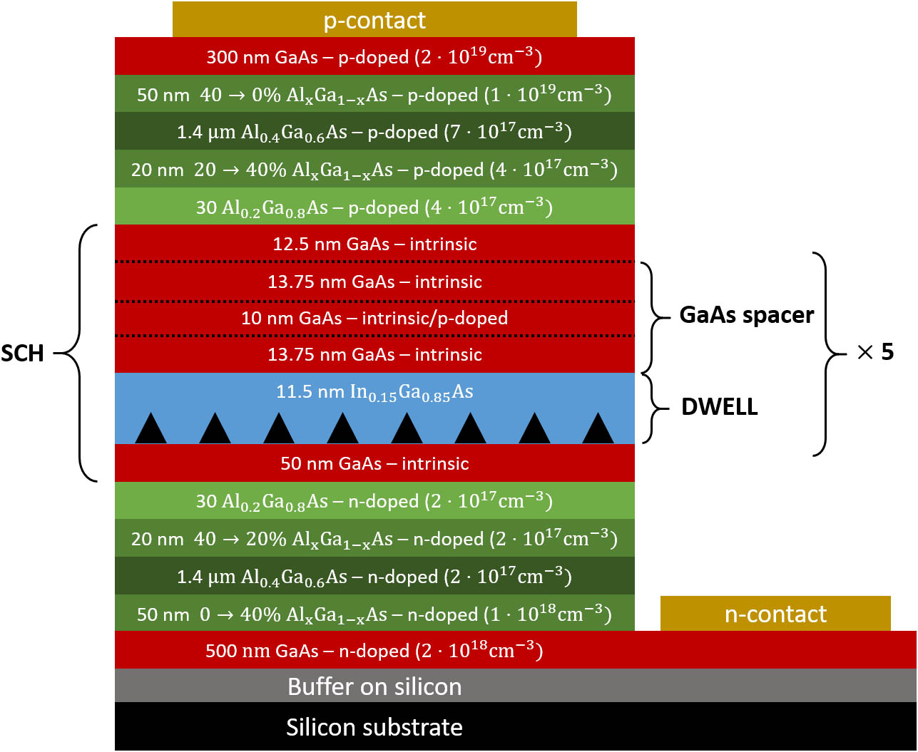
    Schematic representation of the epitaxial structure of the studied QD lasers, similar to those in Refs. [24,25]. The growth direction is from the bottom to the top.
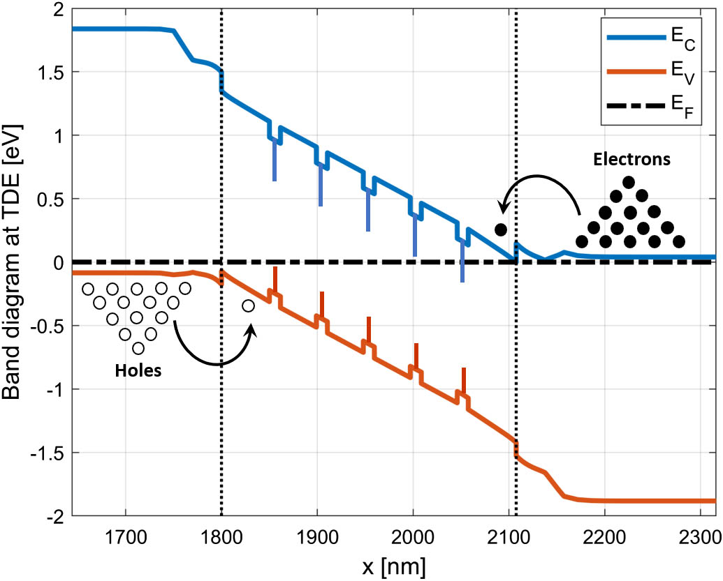
    Fig. 1. Schematic representation of the epitaxial structure of the studied QD lasers, similar to those in Refs. [24,25]. The growth direction is from the bottom to the top.
    Band diagram at thermodynamic equilibrium, with the conduction band (blue), the valence band (red), and the Fermi level (dashed, black). The dotted, vertical lines delimit the SCH region.
    Fig. 2. Band diagram at thermodynamic equilibrium, with the conduction band (blue), the valence band (red), and the Fermi level (dashed, black). The dotted, vertical lines delimit the SCH region.
    Schematic representation of the QD energy states and intersubband transitions.
    Fig. 3. Schematic representation of the QD energy states and intersubband transitions.
    Calculated GS modal gain versus current density for different levels of TDD and experimental gain (circles) from Ref. [24].
    Fig. 4. Calculated GS modal gain versus current density for different levels of TDD and experimental gain (circles) from Ref. [24].
    (a) GS threshold current density and (c) optical power as a function of TDDbulk, for fixed DWELL SRH lifetime corresponding to TDDWL=105 cm−2. The solid lines are almost overlapped. (b) GS threshold current density and slope efficiency and (d) optical power as a function of TDD in the barrier and DWELL layers (TDDWL=TDDbulk).
    Fig. 5. (a) GS threshold current density and (c) optical power as a function of TDDbulk, for fixed DWELL SRH lifetime corresponding to TDDWL=105  cm2. The solid lines are almost overlapped. (b) GS threshold current density and slope efficiency and (d) optical power as a function of TDD in the barrier and DWELL layers (TDDWL=TDDbulk).
    GS (solid) and ES (dotted) optical power with (a) μn=8500 cm2/(V·s) and μp=350 cm2/(V·s) and (b) μn=μp=8500 cm2/(V·s) in the SCH region.
    Fig. 6. GS (solid) and ES (dotted) optical power with (a) μn=8500  cm2/(V·s) and μp=350  cm2/(V·s) and (b) μn=μp=8500  cm2/(V·s) in the SCH region.
    Net capture rate from the bulk states to the WL with (a) μn=8500 cm2/(V·s) and μp=350 cm2/(V·s) and (b) μn=μp=8500 cm2/(V·s) in the SCH region. Layer 1 (5) is the closest to the p-contact (n-contact).
    Fig. 7. Net capture rate from the bulk states to the WL with (a) μn=8500  cm2/(V·s) and μp=350  cm2/(V·s) and (b) μn=μp=8500  cm2/(V·s) in the SCH region. Layer 1 (5) is the closest to the p-contact (n-contact).
    Contribution of (a) electrons and (b) holes to the GS modal gain: solid line is the overall contribution, whereas colored dashed lines are the contribution of the different layers (color legend is the same as in Fig. 6). Vertical lines indicate GS and ES threshold currents. (c) GS electrons and (d) holes occupation probability. The mobility of electrons and holes in the SCH region is μn=8500 cm2/(V·s) and μp=350 cm2/(V·s). Layer 1 (5) is the closest to the p-contact (n-contact).
    Fig. 8. Contribution of (a) electrons and (b) holes to the GS modal gain: solid line is the overall contribution, whereas colored dashed lines are the contribution of the different layers (color legend is the same as in Fig. 6). Vertical lines indicate GS and ES threshold currents. (c) GS electrons and (d) holes occupation probability. The mobility of electrons and holes in the SCH region is μn=8500  cm2/(V·s) and μp=350  cm2/(V·s). Layer 1 (5) is the closest to the p-contact (n-contact).
    GS (solid) and ES (dotted) optical power with (a) no p-type modulation doping and a p-type modulation doping of (b) 5×1017 cm−3 and (c) 30×1017 cm−3.
    Fig. 9. GS (solid) and ES (dotted) optical power with (a) no p-type modulation doping and a p-type modulation doping of (b) 5×10¹⁷  cm3 and (c) 30×1017  cm3.
    (a) GS (blue) and ES (red) threshold current density as functions of the p-type modulation doping density. (b) Total radiative and SRH recombination rates as functions of p-type modulation doping density calculated at the JthGS values in (a).
    Fig. 10. (a) GS (blue) and ES (red) threshold current density as functions of the p-type modulation doping density. (b) Total radiative and SRH recombination rates as functions of p-type modulation doping density calculated at the JthGS values in (a).
    (a) GS modal gain versus current density and (b) holes (GGSmod,p, dashed) and electrons (GGSmod,n, solid) contributions to the modal gain.
    Fig. 11. (a) GS modal gain versus current density and (b) holes (GGSmod,p, dashed) and electrons (GGSmod,n, solid) contributions to the modal gain.
    (a) Contribution of electrons (blue) and holes (red) to the GS modal gain at J=580 A/cm2 versus p-doping density and (b) corresponding GS modal gain.
    Fig. 12. (a) Contribution of electrons (blue) and holes (red) to the GS modal gain at J=580  A/cm2 versus p-doping density and (b) corresponding GS modal gain.
    (a) Conduction band (solid) and electron quasi-Fermi level (dashed) for the bulk states of the SCH region at J=580 A/cm2. (b) Valence band (solid) and hole quasi-Fermi level (dashed) for the bulk states of the SCH region at J=580 A/cm2.
    Fig. 13. (a) Conduction band (solid) and electron quasi-Fermi level (dashed) for the bulk states of the SCH region at J=580  A/cm2. (b) Valence band (solid) and hole quasi-Fermi level (dashed) for the bulk states of the SCH region at J=580  A/cm2.
    Net capture rate from the bulk states to the WL at J=580 A/cm2 for each layer of QDs.
    Fig. 14. Net capture rate from the bulk states to the WL at J=580  A/cm2 for each layer of QDs.
    Total SRH recombination rate versus voltage at three different doping levels. The vertical dashed lines indicate the voltage value corresponding to the lasing threshold.
    Fig. 15. Total SRH recombination rate versus voltage at three different doping levels. The vertical dashed lines indicate the voltage value corresponding to the lasing threshold.
    ParametersValues
    ΔEnk, k=WL,ES,GS [meV]177.7, 30, 41.1 [14]
    ΔEpk, k=WL,ES,GS [meV]166.3, 25, 25 [14]
    τn,CAPBWL, τn,CAPWLES, τn,CAPESGS [ps]0.1, 1, 1 [26]
    τp,CAPBWL, τp,CAPWLES, τp,CAPESGS [ps]0.1, 0.1, 0.1 [26]
    τradk, k=WL,ES,GS [ns]1, 1, 1 [11,22]
    τn,SRHk, k=ES,GS [ns]1, 1 [11,22]
    τp,SRHk, k=ES,GS [ns]1, 1 [11,22]
    QD sheet density NQD,i [cm2]4.9×10¹⁰
    GS (ES) degeneracy μGS (μES)2 (4)
    Gain coefficient G0GS (G0ES) [cm1]433 (779.4)
    Electron (hole) effective mass mn* (mp*) [m0]0.054 (0.49)
    Optical confinement factor Γi2%
    Intrinsic loss αi [cm1]5
    Waveguide width [μm]3.5
    Facet reflection coefficient0.32
    Spontaneous emission factor βsp104
    Group index3.56
    GaAs Dn, Dp [cm2·s1]221, 10
    In0.15Ga0.85AsDn, Dp [cm2·s1]181, 10
    Temperature [K]300
    Table 1. Simulation Parameters
    Marco Saldutti, Alberto Tibaldi, Federica Cappelluti, Mariangela Gioannini. Impact of carrier transport on the performance of QD lasers on silicon: a drift-diffusion approach[J]. Photonics Research, 2020, 8(8): 1388
    Download Citation