• Acta Physica Sinica
  • Vol. 69, Issue 17, 178201-1 (2020)
Xin Zhang1, Xing Chen1, Tian Bai1, Xing-Yan You1, Xin Zhao1, Xiang-Yang Liu2, and Mei-Dan Ye1、3、*
Author Affiliations
  • 1Research Institute for Soft Matter and Biomimetics, College of Physical Science and Technology, Xiamen University, Xiamen 361005, China
  • 2Faculty of Science, National University of Singapore, Singapore 119077, Singapore
  • 3Jiujiang Research Institute of Xiamen University, Jiujiang 332000, China
  • show less
    DOI: 10.7498/aps.69.20200159 Cite this Article
    Xin Zhang, Xing Chen, Tian Bai, Xing-Yan You, Xin Zhao, Xiang-Yang Liu, Mei-Dan Ye. Recent advances in flexible fiber-shaped supercapacitors[J]. Acta Physica Sinica, 2020, 69(17): 178201-1 Copy Citation Text show less
    Numbers of articles on supercapacitors in the past decade.
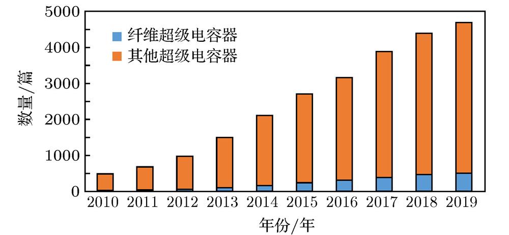
    Fig. 1. Numbers of articles on supercapacitors in the past decade.
    Schematic diagrams of the working mechanism of supercapacitors.
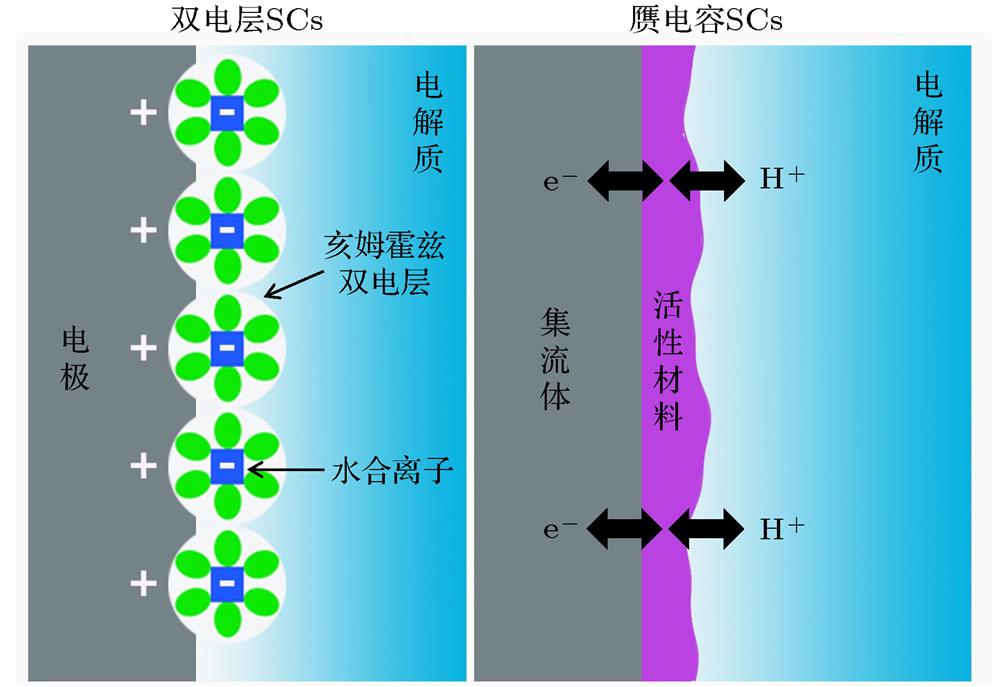
    Fig. 2. Schematic diagrams of the working mechanism of supercapacitors.
    Schematic diagrams of different types of supercapacitors.
    Fig. 3. Schematic diagrams of different types of supercapacitors.
    (a) Schematic diagram of the CVD process in CNT fiber: (b) photographs of a single CF before CVD and CNTs@CF fiber after CVD with diameter of 7.2 mm; (c) photographs of CNTs@CF fibers with diameters of 0.51, 1.20, and 3.64 mm; (d) photos of the cross sectional view and water droplets on cross section and surface of CNTs @CF fiber; (e) photos of a CNTs@CF fiber shrinking after ethanol infiltration and evaporation, and a knotted shrunk fiber[61].
    Fig. 4. (a) Schematic diagram of the CVD process in CNT fiber: (b) photographs of a single CF before CVD and CNTs@CF fiber after CVD with diameter of 7.2 mm; (c) photographs of CNTs@CF fibers with diameters of 0.51, 1.20, and 3.64 mm; (d) photos of the cross sectional view and water droplets on cross section and surface of CNTs @CF fiber; (e) photos of a CNTs@CF fiber shrinking after ethanol infiltration and evaporation, and a knotted shrunk fiber[61].
    (a) Schematic diagrams of the fabricating process for SG-CPF@GF electrodes and FSCs[62]; (b) schematic of the fiber-based supercapacitor; (c) SEM image of the NWs in a plastic wire[63].
    Fig. 5. (a) Schematic diagrams of the fabricating process for SG-CPF@GF electrodes and FSCs[62]; (b) schematic of the fiber-based supercapacitor; (c) SEM image of the NWs in a plastic wire[63].
    (a) Schematic of the fabrication process of the OCNTF; (b) SEM images of pristine CNTF; (c) SEM images of OCNTF; (d) SEM image of PEDOT:PSS@OCNTF; (e) schematic of the fabrication process of the FASC; (f) the structure of the stretchable FASC; (g) schematic of the stretchable FASC; (h) wrapping the CNT fibers around an elastic fiber[41].
    Fig. 6. (a) Schematic of the fabrication process of the OCNTF; (b) SEM images of pristine CNTF; (c) SEM images of OCNTF; (d) SEM image of PEDOT:PSS@OCNTF; (e) schematic of the fabrication process of the FASC; (f) the structure of the stretchable FASC; (g) schematic of the stretchable FASC; (h) wrapping the CNT fibers around an elastic fiber[41].
    (a) Schematic of the ZNCO@Ni(OH)2NWAs on a CNTF; (b), (c) SEM images of ZNCO NWAs/CNTF at different magnifications; (d) SEM image of ZNCO@Ni(OH)2NWAs/CNTF; (e) cross-sectional structure of the CFASCs; (f) wrapping VN@C NWAs/CNTS to the ZNCO@Ni(OH)2NWAs/CNTF/KOH-PVA; (g) CV curves of CFASCs at a scan rate of 25 mV/s with different operating voltages; (h) GCD curves of the CFASCs at a current density of 9 mA/cm2 at voltages from 0.4 to 1.6 V; (i) areal specific capacitance and energy density calculated based on the GCD curves obtained at 9 mA/cm2[69].
    Fig. 7. (a) Schematic of the ZNCO@Ni(OH)2NWAs on a CNTF; (b), (c) SEM images of ZNCO NWAs/CNTF at different magnifications; (d) SEM image of ZNCO@Ni(OH)2NWAs/CNTF; (e) cross-sectional structure of the CFASCs; (f) wrapping VN@C NWAs/CNTS to the ZNCO@Ni(OH)2NWAs/CNTF/KOH-PVA; (g) CV curves of CFASCs at a scan rate of 25 mV/s with different operating voltages; (h) GCD curves of the CFASCs at a current density of 9 mA/cm2 at voltages from 0.4 to 1.6 V; (i) areal specific capacitance and energy density calculated based on the GCD curves obtained at 9 mA/cm2[69].
    (a), (b) SEM images of dandelion-like MNCO NWAs on CNTF at different magnifications; (c) schematic of the fabrication process of FASC[42].
    Fig. 8. (a), (b) SEM images of dandelion-like MNCO NWAs on CNTF at different magnifications; (c) schematic of the fabrication process of FASC[42].
    (a)−(c) SEM images of MNCS NTAs on CNTFs at different magnifications; (d) schematic of MNCS multi-tripod NTAs grown on CNTFs; (e) schematic of the FASC device; (f) CV curves of the FASC device at a scan rate of 30 mV/s with different operating voltages; (g) GCD curves of the FASC at a current density of 2 mA/cm2 from 0.4 to 1.6 V; (h) areal specific capacitance and energy density calculated based on GCD curves obtained at 2 mA/cm2[77].
    Fig. 9. (a)−(c) SEM images of MNCS NTAs on CNTFs at different magnifications; (d) schematic of MNCS multi-tripod NTAs grown on CNTFs; (e) schematic of the FASC device; (f) CV curves of the FASC device at a scan rate of 30 mV/s with different operating voltages; (g) GCD curves of the FASC at a current density of 2 mA/cm2 from 0.4 to 1.6 V; (h) areal specific capacitance and energy density calculated based on GCD curves obtained at 2 mA/cm2[77].
    (a) Schematic of the structural re-arrangement mechanism of PEDOT-S:PSS fiber by the treatment of the sulfuric acid; (b) schematic of the fabrication of PEDOT-S:PSS based T-SFSSs in series; (c) photo of T-SFSSs to lighten up a commercial USB light, the inset photo showing the USB light connected with the T-SFSSs by two twisted PEDOT-S:PSS fibers; (d) photo of T-SFSS consisting of three SFSS in series, with five LEDs lighting up the logo abbreviation (LEDs); (e), (f) photos of a commercial digital watch powered by three connected T-SFSS woven into fabric, each consists of three tandem T-SFSS based on PEDOT-S: PSS fiber; (g) photos of T-SFSS, which includes two SFSS in series to light up the green LED when the strain increases from 0% to 400%[15].
    Fig. 10. (a) Schematic of the structural re-arrangement mechanism of PEDOT-S:PSS fiber by the treatment of the sulfuric acid; (b) schematic of the fabrication of PEDOT-S:PSS based T-SFSSs in series; (c) photo of T-SFSSs to lighten up a commercial USB light, the inset photo showing the USB light connected with the T-SFSSs by two twisted PEDOT-S:PSS fibers; (d) photo of T-SFSS consisting of three SFSS in series, with five LEDs lighting up the logo abbreviation (LEDs); (e), (f) photos of a commercial digital watch powered by three connected T-SFSS woven into fabric, each consists of three tandem T-SFSS based on PEDOT-S: PSS fiber; (g) photos of T-SFSS, which includes two SFSS in series to light up the green LED when the strain increases from 0% to 400%[15].
    (a) Schematic of the fabrication process and microscopic structure of the ternary coaxial fibers; (b)−(d) SEM images of GCP@CMC; (e) cycling stability of GCP@CMC at 3.0 mA/cm2 after 5000 cycles; (f) bending stability test, illustration showing different bending states; (g) plots compared with selected fiber supercapacitor; (h) photograph of three bending FSCs assembled by GCP@CMC in series; (i) LED lit by three FSCs assembled GCP@CMC in series[43].
    Fig. 11. (a) Schematic of the fabrication process and microscopic structure of the ternary coaxial fibers; (b)−(d) SEM images of GCP@CMC; (e) cycling stability of GCP@CMC at 3.0 mA/cm2 after 5000 cycles; (f) bending stability test, illustration showing different bending states; (g) plots compared with selected fiber supercapacitor; (h) photograph of three bending FSCs assembled by GCP@CMC in series; (i) LED lit by three FSCs assembled GCP@CMC in series[43].
    (a) Schematic of ion and charge transfer in the NPN electrode; (b) schematic of the preparation of the CMF; (c)−(e) SEM images of the CMF at different magnifications[16].
    Fig. 12. (a) Schematic of ion and charge transfer in the NPN electrode; (b) schematic of the preparation of the CMF; (c)−(e) SEM images of the CMF at different magnifications[16].
    Schematic of the fabrication process of forest-like NiO NSs@CNTs@CuO NWAs/Cu fibers by waste cable wires[84].
    Fig. 13. Schematic of the fabrication process of forest-like NiO NSs@CNTs@CuO NWAs/Cu fibers by waste cable wires[84].
    (a) CoS2 system; (b) P-CoS2 system; (c), (d) local charge density distributions of CoS2 and P-CoS2; (e), (f) CoS2 and Co-location of cobalt in (100) plane of P-CoS2. A side view of the crystalline structure of which cobalt is shown in blue, sulfur is pink, phosphorus is green, oxygen is red, and hydrogen is yellow[86].
    Fig. 14. (a) CoS2 system; (b) P-CoS2 system; (c), (d) local charge density distributions of CoS2 and P-CoS2; (e), (f) CoS2 and Co-location of cobalt in (100) plane of P-CoS2. A side view of the crystalline structure of which cobalt is shown in blue, sulfur is pink, phosphorus is green, oxygen is red, and hydrogen is yellow[86].
    (a)−(c) photographs of the fiber-shaped supercapacitors at increasing bending angles; (d) the NPCM-FSC floats on water; (e)−(h) photos of the red LED lighted by NPCM-FSC; (i), (j) the application of the as-assembled NPCM-FSC; (k) schematic of the fabrication process of FSC[16].
    Fig. 15. (a)−(c) photographs of the fiber-shaped supercapacitors at increasing bending angles; (d) the NPCM-FSC floats on water; (e)−(h) photos of the red LED lighted by NPCM-FSC; (i), (j) the application of the as-assembled NPCM-FSC; (k) schematic of the fabrication process of FSC[16].
    (a) Schematic of the fabrication process of the FSC device; (b) schematic diagram of the FTENG; (c) basic working mecha-nism of the FTENG; (d) circuit diagram of the self-charging power system and load; (e) charging/discharging curves of the as-prepared FSCs charged by the FTENG[18].
    Fig. 16. (a) Schematic of the fabrication process of the FSC device; (b) schematic diagram of the FTENG; (c) basic working mecha-nism of the FTENG; (d) circuit diagram of the self-charging power system and load; (e) charging/discharging curves of the as-prepared FSCs charged by the FTENG[18].
    (a) Photo of the fiber asymmetric supercapacitor; (b) CV curves; (c) GCD curves; (d) the volume capacitance increases with the potential window of the asymmetric supercapacitor; (e) schematic of the device, current response of a photodetector powered by a FASC; (f) illuminated at different incident light intensities; (g) different bending states under a light intensity of 40 mW/cm2[90].
    Fig. 17. (a) Photo of the fiber asymmetric supercapacitor; (b) CV curves; (c) GCD curves; (d) the volume capacitance increases with the potential window of the asymmetric supercapacitor; (e) schematic of the device, current response of a photodetector powered by a FASC; (f) illuminated at different incident light intensities; (g) different bending states under a light intensity of 40 mW/cm2[90].
    (a) Schematic of integrated linear device for photoelectric conversion (PC) and energy storage (ES); (b), (c) SEM images of oriented titanium dioxide nanotubes grown on Ti wires by electrochemical anodization for 2 h at low and high magnifications, respectively; (d), (e) SEM images of CNT fibers at low and high magnifications, respectively; (f) schematic of working mechanism, CB = conduction band, VB = valence band; (g) typical current density/voltage curve under AM 1.5 light; (h), (i) schematic diagram of circuit connection during charging and discharging respectively; (j) typical energy wire light discharge curve. Discharge current is 0.1 mA[93].
    Fig. 18. (a) Schematic of integrated linear device for photoelectric conversion (PC) and energy storage (ES); (b), (c) SEM images of oriented titanium dioxide nanotubes grown on Ti wires by electrochemical anodization for 2 h at low and high magnifications, respectively; (d), (e) SEM images of CNT fibers at low and high magnifications, respectively; (f) schematic of working mechanism, CB = conduction band, VB = valence band; (g) typical current density/voltage curve under AM 1.5 light; (h), (i) schematic diagram of circuit connection during charging and discharging respectively; (j) typical energy wire light discharge curve. Discharge current is 0.1 mA[93].
    基底优点缺点
    碳基纤维功率密度高、充放电速率快、循环寿命长延展性差、成本高、制备工艺复杂
    聚合物纤维延展性和拉伸性能优异电容低、循环性差
    金属纤维成本低廉、制备简单、机械强度高、电导率高柔韧性、拉伸性能较差
    水凝胶纤维良好的拉伸形变能力空气中易脱水、电容较低
    尼龙纤维等来源广泛易制备、部分纤维有拉伸性能电容和循环性较差
    Table 1.

    Advantages and disadvantages of different fiber substrates.

    不同类型纤维基底的优缺点

    Xin Zhang, Xing Chen, Tian Bai, Xing-Yan You, Xin Zhao, Xiang-Yang Liu, Mei-Dan Ye. Recent advances in flexible fiber-shaped supercapacitors[J]. Acta Physica Sinica, 2020, 69(17): 178201-1
    Download Citation