H. Alisafaee1, J. Marmon2, and M. A. Fiddy1,3,*
Abstract
Coupled plasmonic nanoparticles of Au and nanorods of ZnTe are modeled and fabricated. Full-wave simulation is performed to obtain an optimum design for enhanced light absorption and to explain scattering properties of the structure. The fabrication method of such arrays is described. Modeling the spectral properties using equivalent circuit theory is also implemented to provide an intuitive approach regarding the design of optical metamaterials with predetermined properties.1. INTRODUCTION
ZnTe is an interesting II–VI semiconductor material used in optoelectronic devices, such as in photovoltaic elements [1,2], green light-emitting diodes [3], broad-frequency field sensors [4,5], waveguides [6,7], and gain media [8,9]; some of these devices take advantage of nanoscale effects [10]. ZnTe also has nonlinear optical properties [11]. This material has been widely used because it is relatively easy to p-dope compared to other II–VI materials [12,13]. Two wide-bandgap materials configured as a type II heterojunction, such as a ZnTe/ZnO core–shell structure, could be used to achieve an ideal effective bandgap for solar cells [14], thereby exploiting both the optical coupling between the two components and unique electrical properties. Moreover, a vertical nanorod array of this structure improves light trapping and potentially reduces charge diffusion lengths, hence further increasing photovoltaic efficiency [15–17]. To grow these ZnTe nanorods, it is possible to utilize gold nanoparticles to catalyze the growth via the vapor–liquid–solid mechanism [18].
Noble metals such as gold and silver, or transparent conductive oxides, e.g., ITO and AZO, are known to exhibit plasmon oscillations when illuminated by light. During these oscillations, confined conduction electrons can be driven by the electric field of light into a resonant condition that is dependent on different parameters, such as material, size, shape, and host medium properties [19]. In the case of spherical nanoparticles of size and permittivity in a host medium with permittivity , light scattering and absorption cross sections are defined by [20]: where is the wavenumber of light. At the plasmon resonance condition scattering and absorption maxima occur, assuming the imaginary parts of the permittivities are small. In the case of small particles with a loss term in their permittivity, the absorption dominates over scattering. A discrete dipole approximation may also be applied to study the interactions in the quasi-static regime, that is, when the wavelength of light is much larger than the size of the nanoparticles [21].
The plasmonic structures we introduce here are ideally vertical arrays composed of gold nanospheres sitting on top of ZnTe nanorods. We numerically investigate the spectral response of these plasmonic Au–ZnTe nanostructures and find the effects of array structure parameters on the extinction of light. We use the finite element method (FEM) to explore the best design for such a nanostructure array. This composite structure can also be modeled as a metamaterial composed of distinct nanocircuit elements [22,23], which means that each nanostructure element can be represented by a nanoresistor, nanocapacitor, or nanoinductor, or a combination of them. Therefore, one can intuitively study the effects of design parameters simply by studying the circuit elements. Finally, we explain the method of fabrication of such composite plasmonic structures.
Sign up for Photonics Research TOC. Get the latest issue of Photonics Research delivered right to you!Sign up now
2. MODELING
Using COMSOL as our FEM modeling tool, we designed a unit cell of coupled plasmonic Au–ZnTe structure, where a gold nanosphere sits upon a ZnTe nanorod (see Fig. 1 inset). The unit cell includes a gold nanosphere of size 100 nm and a nanorod of diameter and length 60 and 500 nm, respectively. Linearly polarized light is assumed incident from above the unit cell. Parallel to the axis of the nanorod shown in Fig. 1, and in both directions, we employed Floquet boundary conditions to account for neighboring nanorod structures that can contribute to coupling effects in the computation process. In this way, we can simulate an infinite two-dimensional array of nanostructure elements that replicate the unit cell. Material properties of ZnTe and Au can be found everywhere, e.g., Refs. [11] and [24], respectively.
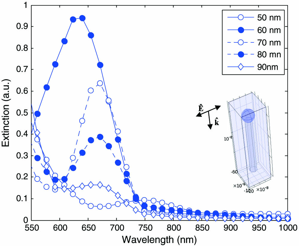
Figure 1.Extinction spectra of incident light as functions of the spacing between nanorod structures. The Au diameter is 100 nm, and the ZnTe diameter and length are 60 and 500 nm, respectively. The inset shows the unit cell of simulation.
We investigate the spectral properties of this initial design upon changes in different parameters to find a suitable set of final parameters in order to guide the fabrication and predict the results of the optical experiments. Two of the main parameters that can be controlled in the fabrication process are (1) the spacing between the adjacent plasmonic nanorods and (2) the length of the ZnTe rods. The extinction spectra for a variety of reasonable spacing values are calculated and shown in Fig. 1. It can be seen that the optical response of the structure is fairly sensitive to the spatial distribution of the nanostructure array, and there is an enhanced extinction in the wavelength range 550–700 nm at 60 nm spacing. Since the extinction is defined as the sum of the absorption and the scattering, one can expect enhanced absorption or scattering, or even both. Enhanced scattering, when directed toward the absorptive material, can help to increase light–matter interaction, which would eventually lead to an increase in the total absorption. This is a very important feature of this structure for use in applications such as solar harvesting or detectors.
Regarding the extinction peaks of Fig. 1, it can be speculated that one of the main reasons for such an increase in the extinction is a reduction in the reflectivity of the structure. Therefore, light scattering and absorption occur more at some spacing values. Further, to explain other origins of these peaks at these optimal parameters, different processes could be taken into account. A mechanism that is common in all of the situations, and is considerable at wavelengths in the range 550–650 nm compared to longer wavelengths, is the pronounced localized surface plasmon resonance (LSPR) of the gold nanospheres. The LSPR can result in enhanced light–matter interaction through two methods; the first one is the increased forward scattering from the gold sphere to the single nanorod that is attached to it, and the second method is the increased side scattering that adds to the amount of forward-scattered light in the adjacent nanorods. This LSPR mechanism is also dependent on the spacing between nanoelements. Another mechanism that affects absorption and dependence on the length of the nanorods is the dielectric resonance due to interference. That is, when the optical length of the nanorod approximately matches the odd multiples of a quarter-wavelength (, ), one can expect increased field in the structure, and vice versa. For example, with at , the optical thickness is 493.5 nm, and hence a destructive interference is expected, resulting in lower absorption, as can be seen in Fig. 1. However, the peak for 60 nm spacing is not obeying this rule, which suggests the existence of another dominant mechanism. The last mechanism for such extinction peaks includes the effects of both length and spacing, such that the overlap between the scattered light and the neighboring nanorods is effectively higher at some conditions, resulting in an efficient secondary absorption. This could be the main reason behind the large peak at 60 nm spacing, after ruling out forward scattering. Therefore, it is the competition and collaboration between these mechanisms that lead to such different peaks as the length and the spacing parameters of the structure change. Also, as is obvious from extrapolation of all the curves to wavelengths shorter than 550 nm, a high extinction regime exists, due to natural absorption of the materials.
Figure 2 demonstrates the power dissipation of light in the nanorod structures. Here, the spacing is 60 nm and the length is 500 nm. The different spectral responses of light absorption in the gold nanosphere and ZnTe nanorod are observable from this figure. One can easily spot the high absorption localizations in the ZnTe rod [Figs. 2(c) and 2(d)]. There is also a high absorption region close to the top of the ZnTe. This can be from the resonant forward scattering of the gold due to the LSPR effect, which, as mentioned earlier, directly helps the absorption. To confirm this, we computed the scattering profile of a nanocomposite element [Figs. 2(e) and 2(f)]. The forward scattering into the nanorod and also the side scattering to the neighboring nanorods can be verified. Also, the effects of coupling between nanostructures in the directions parallel and perpendicular to the polarization plane of light is observable in these patterns. Therefore, it is now clear that the gold nanospheres can be utilized in a multipurpose procedure; one purpose is to help the growth of the ZnTe nanorods through catalyzing the fabrication process, the second is to control the diameter of nanorods, and the third is to facilitate absorption through forward and side scattering.

Figure 2.Power dissipation in the plasmonic nanorod structure as a function the light wavelength: (a) 1000 nm, (b) 750 nm, (c) 600 nm, (d) 550 nm. The neighboring nanorods are placed with a spacing of 60 nm. Scattering profiles of the Au–ZnTe element at for directions (e) perpendicular and (f) parallel to the polarization plane of light.
We also considered the effects of nanorod length on the spectral response of our plasmonic structure (Fig. 3). The spacing is 60 nm. For comparison purposes, since the lengths are different, the extinction values are normalized by dividing them to the volume of the nanorod in order to obtain a measure of effective extinction. The results show spectral sensitivity depending on the length of the ZnTe nanorod. The majority of these variations can be due to spatial overlap with the side lobes of the LSPR scattering. It can be seen that the length of 250 nm provides the best extinction over the spectral region where the absorption of ZnTe is relatively higher. To investigate the absorption inside the nanorod, we separate the contribution of the gold from the extinction spectra and study the two main wavelengths where the absorption coefficient of the ZnTe is larger. The results are shown in Fig. 4. We have found that a huge increase in the amount of absorption at wavelengths of 550 and 600 nm occurs when the nanorod length is around 250 nm. This can be considered the optimal length for our structure. The insets of Fig. 4 show the distribution of absorption throughout the nanorods. We can see that an effective absorption can be achieved in all the nanorods by carefully designing the spacing and length of the array structure. We also studied another case, when no gold was attached on top of the ZnTe nanorod. This study helps to understand the important role of gold in the enhancement of absorption. The results for the same two wavelengths are plotted in Fig. 4. The enhancement factor, which we define as the ratio of the absorption with the gold nanosphere to the absorption without it, rises to 8 for the optimal length we found earlier.
Figure 3.Normalized extinction spectra as a function of nanorod length with a constant 60 nm spacing between structures.
Figure 4.Power dissipation (filled) and enhancement factor (empty) versus ZnTe length at wavelengths of 600 (diamonds) and 550 nm (circles). Insets: absorption distribution at 550 (left) and 600 nm (right).
3. LCR CIRCUIT MODEL
At our wavelength range of interest, the real parts of the permittivity of Au and ZnTe are, respectively, negative and positive. They can be modeled as lumped circuit elements having an inductance () and a capacitance () response, respectively. Therefore, we can use an equivalent circuit to model the response of not only a single nanostructure but also an array of such nanostructures. Figure 5 shows such a circuit model. The resistors represent the material’s losses. We assume a square lattice of such structures and add capacitors and to account for spacing between the spheres and rods, respectively. Since the spacing between the spheres is on the order of their radii, they can be coupled together. But for nanorods, the spacing is about three times larger than the radius. Thus, we neglect the coupling between them.
Figure 5.(a) Schematic of Au–ZnTe array with equivalent circuit model elements and (b) calculation of the induced relative dipole moment in the gold spheres. The white line is the LSPR in air for and isolated sphere. (c) Comparison of LCR circuit response and simulation data points for a 60 nm separated array of Fig. 1.
Applying the approach of Ref. [23] to obtain the equivalent values of circuit elements, we find fH (inductance of sphere), aF(fringe capacitance of sphere), fF(capacitance of rod), aF (fringe capacitance of rod), and the total values for the LCR circuit would be fH, aF, and . This is a bandpass filter with a factor of 7.78 and fractional bandwidth of 0.1288, centered at a frequency corresponding to a 630 nm light.
The bandwidth of the resonance is about 80 nm. These characteristics approximately match the spectral properties of Fig. 1 (60 nm spacing). The plot of such a response is shown in Fig. 5 together with the simulation points of Fig. 1. To compare the results of LCR and FEM, it should be noted that the LCR approach is a quasi-static approximation that is independent of the wavelength. We used the optical properties of the materials at 630 nm. Any deviations in the optical properties result in deviations in the spectrum, particularly at longer wavelengths. Another source of error in the use of the LCR method arises from neglecting the retardation effects. The structure we are using here is comparable to the wavelength of the incident light, which dictates that retardation effects should be taken into account.
We have investigated the coupling of gold spheres using this LCR method and concluded that only those spheres aligned in the polarization of light can be coupled efficiently. The coupling induces a dipole in each sphere, whose magnitude is dependent on the distance between the spheres. In Fig. 5, we have calculated this dipole moment compared to the local dipole response of the sphere in response to the incident light. As is obvious, the coupling is strong only at a close proximity, and it can shift the resonance of the LSPR to the red. However, with the geometrical parameters we used for the simulation, there is unlikely to be a redshift from the LSPR coupling when referring to these calculations. Nevertheless, one can easily and intuitively figure out that both the circuits of the sphere and the rod are coupled together, and the capacitor response of the rod affects the resonance frequency of the sphere such that the total capacitance is increased, which results in a redshift in the resonance of the structure.
4. FABRICATION
Here we only report the fabrication procedure and its resulting structures. Au–ZnTe nanostructures were fabricated in several steps. First, a thin film of gold was sputtered onto an Si(111) wafer. Then the wafer was thermally annealed to create Au islands. The Au thin films on the Si(111) wafers were heated to 600°C, 625°C, 650°C, or 700°C over 30 min and held at this temperature for 1 h and then allowed to cool naturally. Sputtering thicknesses from 1 to 10 nm were investigated, but only thicknesses above 5 nm resulted in measurable Au islands. Based on these capabilities, we were able to create Au islands with a size range of about 100 nm that consequently resulted in a narrower diameter for the ZnTe nanorods. We should note that the Au dimensions directly control the growth of the ZnTe nanorod diameter. Finally, the Au islands were used to catalyze ZnTe growth in a chemical vapor deposition process to create the Au–ZnTe structures. To investigate the sample, we used dark field microscopy to observe the LSPR and spacing between the composite elements (Fig. 6). Characterization of electrical and optical properties of this structure is beyond the scope of this work and will be reported separately.
Figure 6.Scanning electron microscope image of the large-scale fabricated composite nanostructure. The scale bar is 10 μm. Insets show a dark field image of the Au islands (left) and selected nanostructure elements at 200 nm scale (right).
5. CONCLUSIONS
We have studied the spectral properties of a composite plasmonic array structure made from gold nanospheres and ZnTe nanorods. For applications in solar harvesting and detectors, we investigated the effects of structural parameters on light absorption and scattering. We found an optimum design for nanorod length and array spacing that can provide enhanced extinction. Moreover, we used an LCR equivalent circuit model to intuitively study the response of our proposed structure. One of the main conclusions of our work is the role of the plasmonic gold spheres incorporated into our design. We found that the gold has a few benefits: one is to help during fabrication in the growth of the ZnTe nanorods, and another is to provide more absorption in the ZnTe nanorods through LSPR. The results of these studies are of great importance in developing novel devices for solar harvesting and detectors.
References
[1] S. Wang, D. Ding, X. Liu, X.-B. Zhang, D. J. Smith, J. K. Furdyna, Y. H. Zhang. MBE growth of II–VI materials on GaSb substrates for photovoltaic applications. J. Cryst. Growth, 311, 2116-2119(2009).
[2] Y.-H. Zhang, S.-Q. Yu, S. R. Johnson, D. Ding, S.-N. Wu. A proposal of monolithically integrated multijunction solar cells using lattice-matched II/VI and III/V semiconductors. Proceedings of the 33rd IEEE Photovoltaic Energy Specialist Conference, 1-5(2008).
[3] K. Sato, M. Hanafusa, A. Noda, A. Arakawa, M. Uchida, T. Asahi, O. Oda. ZnTe pure green light-emitting diodes fabricated by thermal diffusion. J. Cryst. Growth, 214, 1080-1084(2000).
[4] Q. Zhang, J. Zhang, M. I. B. Utama, B. Peng, M. de la Mata, J. Arbiol, Q. Xiong. Exciton-phonon coupling in individual ZnTe nanorods studied by resonant Raman spectroscopy. Phys. Rev. B, 85, 085418(2012).
[5] Q. Wu, M. Litz, X.-C. Zhang. Broadband detection capability of ZnTe electro-optic field detectors. Appl. Phys. Lett., 68, 2924-2926(1996).
[6] S. Valette, G. Labrunie, J. Lizet. Optical waveguides in ion-implanted ZnTe. J. Appl. Phys., 46, 2731-2732(1975).
[7] Y. Kumagai, M. Kobayashi. Growth of ZnMgTe/ZnTe waveguide structures and analysis of the light polarization with the electric field. Jpn. J. Appl. Phys., 51, 02BH06(2012).
[8] L. D. De Loach, R. H. Page, G. D. Wilke, S. A. Payne, W. F. Krupke. Transition metal-doped zinc chalcogenides: spectroscopy and laser determination of a new class of gain media. IEEE J. Quantum Electron., 32, 885-895(1996).
[9] F. A. Majumder, C. Klingshirn, R. Westphäling, H. Kalt, A. Naumov, H. Stanzi, W. Gebhardt. Grain processes in ZnTe epilayers on GaAs. Phys. Status Solidi B, 186, 591-599(1994).
[10] M. S. Litz, D. C. Judy, N. Tesny. A ZnTe electro-optic electric field sensor. Proc. SPIE, 3702, 30-35(1999).
[11] H. H. Li. Refractive index of ZnS, ZnSe, ZnTe and its wavelength and temperature derivatives. J. Phys. Chem. Ref. Data, 13, 103-150(1984).
[12] W. I. Wang. The problem of doping wide gap II–VI compound semiconductors and its solutions. MRS Proc., 228, 319-326(1991).
[13] U. V. Desnica. Doping limits in II–VI compounds—challenges, problems and solutions. Prog. Cryst. Growth Charact. Mater., 36, 291-357(1998).
[14] Y. Zhang, L.-W. Wang, A. Mascarenhas. Quantum coaxial cables for solar energy harvesting. Nano Lett., 7, 1204-1269(2007).
[15] M. M. Adachi, M. P. Anantram, K. S. Karim. Core-shell silicon nanowire solar cells. Science Rep., 3, 1546(2013).
[16] Z. Li, J. Wang, N. Singh, S. Lee. Optical and electrical study of core-shell silicon nanowires for solar applications. Opt. Express, 19, A1057-A1066(2011).
[17] Y. Cao, Z. Wu, J. Ni, W. A. Bhutto, J. Li, S. Li, K. Huang, J. Kang. Type-II core/shell nanowire heterostructures and their photovoltaic applications. Nano-Micro Lett., 4, 135-141(2012).
[18] R. S. Wagner, W. C. Ellis. Vapor-liquid-solid mechanism of single crystal growth. Appl. Phys. Lett., 4, 89-90(1964).
[19] K. L. Kelly, E. Coronado, L. Zhao, G. C. Schatz. The optical properties of metal nanoparticles: the influence of size, shape, and dielectric environment. J. Phys. Chem. B, 107, 668-677(2003).
[20] S. A. Maier. Plasmonics: Fundamentals and Applications(2007).
[21] P. J. Flatau, B. T. Draine. Discrete-dipole approximation for scattering calculations. J. Opt. Soc. Am. A, 11, 1491-1499(1994).
[22] A. Alú, A. Salandrino, N. Engheta. Coupling of optical lumped nanocircuit elements and effects of substrates. Opt. Express, 15, 13865-13876(2007).
[23] C. Huang, X. Yin, H. Huang, Y. Zhu. Study of plasmon resonance in a gold nanorod with an LC circuit model. Opt. Express, 17, 6407-6413(2009).
[24] P. B. Johnson, R. W. Christy. Optical constants of the noble metals. Phys. Rev. B, 6, 4370-4379(1972).


