• Photonics Research
  • Vol. 9, Issue 9, 1854 (2021)
Hai-Xiao Wang1、4、†,*, Li Liang1、†, Bin Jiang2, Junhui Hu1, Xiancong Lu3, and Jian-Hua Jiang2、5、*
Author Affiliations
  • 1School of Physical Science and Technology, Guangxi Normal University, Guilin 541004, China
  • 2School of Physical Science and Technology, Collaborative Innovation Center of Suzhou Nano Science and Technology, Soochow University, Suzhou 215006, China
  • 3Department of Physics, Xiamen University, Xiamen 361005, China
  • 4e-mail: hxwang@gxnu.edu.cn
  • 5e-mail: jianhuajiang@suda.edu.cn
  • show less
    DOI: 10.1364/PRJ.433188 Cite this Article Set citation alerts
    Hai-Xiao Wang, Li Liang, Bin Jiang, Junhui Hu, Xiancong Lu, Jian-Hua Jiang. Higher-order topological phases in tunable C3 symmetric photonic crystals[J]. Photonics Research, 2021, 9(9): 1854 Copy Citation Text show less

    Abstract

    We demonstrate that multiple higher-order topological transitions can be triggered via the continuous change of the geometry in kagome photonic crystals composed of three dielectric rods. By tuning a single geometry parameter, the photonic corner and edge states emerge or disappear with higher-order topological transitions. Two distinct higher-order topological insulator phases and a normal insulator phase are revealed. Their topological indices are obtained from symmetry representations. A photonic analog of the fractional corner charge is introduced to distinguish the two higher-order topological insulator phases. Our predictions can be readily realized and verified in configurable dielectric photonic crystals.

    1. INTRODUCTION

    Topological phases and phase transitions have been extensively studied in electronic [1,2], photonic [3], and acoustic [4,5] systems in the past decades. Recently, a new class of topological insulators, called higher-order topological insulators (HOTIs) that are characterized by higher-order bulk-boundary (e.g., bulk-corner or bulk-hinge) correspondence, were discovered [636]. HOTIs set up examples with multidimensional topological physics going beyond the bulk-edge correspondence in conventional topological insulators and semimetals and thus attract growing attention. Prototype HOTIs include quadrupole and octupole topological insulators [616,37,38], 3D HOTIs in electronic systems with topological hinge states [1720], and HOTIs with quantized Wannier centers [2134,3941]. Among these prototype HOTIs, the breathing kagome lattice is regarded as an excellent platform to study higher-order topological phases and phase transitions. It was first proposed in Ref. [21], and subsequently experimentally realized in acoustic [22,23] and photonic [24,25] systems. In the breathing kagome lattice, the higher-order topology is characterized by the quantized bulk polarization (or the position of the Wannier center). When there is a mismatch between the Wannier center and the lattice site, the breathing kagome lattice becomes a higher-order topological phase and exhibits gapped edge states and in-gap corner states. On the contrary, the breathing kagome lattice becomes a topological trivial phase when the Wannier center overlaps with the lattice site. Despite extensive studies on HOTIs based on the breathing kagome lattice, most studies only distinguish the higher-order topological phases from the trivial phases. As a result, the distinctions between two higher-order topological phases and phase transitions have not yet been revealed.

    Here, we study multiple higher-order topological phases and phase transitions in C3 symmetric 2D photonic crystals (PhCs). We show that by moving the dielectric rods continuously, the C3 symmetric PhCs can switch between triangle and kagome lattice configurations, leading to rich higher-order topological phases and phase transitions. Accompanying such phase transitions, the corner and edge states emerge or disappear, while the corner charge changes between 0 and 1/3. The topological indices for various phases are deduced from the symmetry indicators that are closely related to the fractional corner charge [42]. We also discuss the physical meaning of the fractional corner charge in the photonic context. The richness of the higher-order topological phases and their evolutions provide intriguing photonic phenomena and potential applications in topological photonics that can be readily realized in genuine materials.

    2. HIGHER-ORDER TOPOLOGICAL PHASES IN TUNABLE C3 symmetric photonic crystals

    We study 2D hexagonal PhCs of C3 rotation symmetry, as illustrated in Fig. 1. The lattice vectors are denoted as a1=(a,0) and a2=(a2,3a2), where a is the lattice constant. The side length of the unit cell is denoted as l=a/3. Throughout this study, we consider the C3 symmetric PhC to consist of three identical dielectric rods with permittivity ϵ=15 and radii r=0.1a. The simplest configuration is the triangular lattice with a dielectric rod at the center of each unit cell [Fig. 1(a)], which can be regarded as a special case where three identical dielectric rods overlap with each other. By moving the three dielectric rods along the three symmetry lines, as indicated by the arrows in Fig. 1(b), the PhC undergoes a continuous geometry transformation that includes three triangular lattice configurations (denoted as triangular I, II, and III) and three kagome lattice configurations (denoted as kagome I, II, and III), as shown in Figs. 1(b)–1(f). The configurations between these six special cases are the breathing kagome lattices. The whole cycle of the continuous deformation encompasses d from 0 to 3l, as shown in Fig. 1. The kagome lattices are characterized by d=(n+12)l with n=0,1,2, while the triangular lattices are characterized by d=nl with n=0,1,2.

    Geometric transitions in 2D PhCs with C3 symmetry. The primitive cells are indicated by hexagonal dotted lines with the lattice constant a and the side length l. A tunable parameter d with a range of 0–3l (the parameter d is modulo 3l) is employed to illustrate the geometric transitions between triangular, kagome, and breathing kagome configurations. By tuning the geometric parameter d, the C3 symmetry is preserved, while various configurations can be generated, including: (a) triangular I with d=0/d=3l, (b) kagome I with d=0.5l, (c) triangular II with d=l, (d) kagome II with d=1.5l, (e) triangular III with d=2l, and (f) kagome III with d=2.5l. Each primitive cell consists of three dielectric rods (possibly overlapping with each other) with identical radii r=0.1a and permittivity ϵ=15. (g) Possible position of the Wannier center for C3 symmetric unit cells.

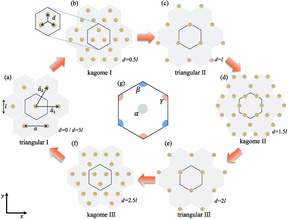
    Figure 1.Geometric transitions in 2D PhCs with C3 symmetry. The primitive cells are indicated by hexagonal dotted lines with the lattice constant a and the side length l. A tunable parameter d with a range of 0–3l (the parameter d is modulo 3l) is employed to illustrate the geometric transitions between triangular, kagome, and breathing kagome configurations. By tuning the geometric parameter d, the C3 symmetry is preserved, while various configurations can be generated, including: (a) triangular I with d=0/d=3l, (b) kagome I with d=0.5l, (c) triangular II with d=l, (d) kagome II with d=1.5l, (e) triangular III with d=2l, and (f) kagome III with d=2.5l. Each primitive cell consists of three dielectric rods (possibly overlapping with each other) with identical radii r=0.1a and permittivity ϵ=15. (g) Possible position of the Wannier center for C3 symmetric unit cells.

    Intuitively, as the dielectric rods move, the Wannier center changes. We consider the band gap between the first and the second photonic bands; therefore, there is only one Wannier center in the unit cell that can locate at the center (α) or the corner of the unit cell (β or γ), as shown in Fig. 1(g). The Wannier center positions of the triangular lattices with different configurations are discussed in detail in Appendix A. Unlike the positions of the dielectric rods, the Wannier center is constrained by the crystalline symmetry and thus cannot continuously change. The change of the Wannier center is nonadiabatic, which must be achieved by the closing and reopening of the band gap, as shown in detail below.

    We first provide the photonic band structures for nine prototype cases in Figs. 2(a)–2(c), where we use c/a as the frequency unit (c is the speed of light in vacuum). Throughout this work, we focus on the low-lying photonic bands due to the transverse magnetic (TM) harmonic modes. All the numerical simulations are carried out using the finite element numerical solver COMSOL Multiphysics. The photonic bands for the triangular I, II, and III configurations are shown in Fig. 2(a), which indicates that the three triangular configurations have an identical band structure. This phenomenon happens because the three triangular configurations differ only by a partial lattice translation, while the structure of the 2D array of the dielectric rods remains the same. However, the symmetry representations of the photonic bands are distinct for the three triangular configurations. Hence, their topological properties are different. In particular, the location of the Wannier center is distinct for the three triangular configurations, as revealed below.

    Photonic band structures of 2D PhCs with C3 symmetry for: (a) d=0,l,2l (i.e., triangular I, II, and III lattices), (b) d=0.5l,1.5l,2.5l (i.e., kagome I, II, and III lattices), and (c) d=0.25l,1.25l,2.25l (i.e., breathing kagome lattices). (d) The eigenfrequencies of the first and second photonic bands at the K point as functions of d. Band gaps of distinct topology are painted with different colors. The topological index χ is labeled for each region. The Wannier center for each region also is depicted. Insets illustrate the phase distributions of the eigenstates of the first photonic band at the K point for various d.

    Figure 2.Photonic band structures of 2D PhCs with C3 symmetry for: (a) d=0,l,2l (i.e., triangular I, II, and III lattices), (b) d=0.5l,1.5l,2.5l (i.e., kagome I, II, and III lattices), and (c) d=0.25l,1.25l,2.25l (i.e., breathing kagome lattices). (d) The eigenfrequencies of the first and second photonic bands at the K point as functions of d. Band gaps of distinct topology are painted with different colors. The topological index χ is labeled for each region. The Wannier center for each region also is depicted. Insets illustrate the phase distributions of the eigenstates of the first photonic band at the K point for various d.

    Similarly, the photonic band structures for the kagome I, II, and III configurations are identical because they can be related to each other by partial lattice translations, as shown in Fig. 2(b). Such translations change the location of the Wannier center as well as the symmetry representations of the Bloch bands and their topological properties.

    Furthermore, as shown in Fig. 2(d), the photonic band structure is identical, if two configurations differ by an integer time of l in the geometry parameter d. Since the lattice periodicity for the translation along the black arrows in Fig. 1(b) is 3l, there are three different configurations with the same photonic band structure, where the geometry parameter d differs by an integer time of l. The translation of l along the black arrows in Fig. 1(b) shifts the unit cell center to the unit cell corner without changing the pattern of the 2D array of the dielectric rods. The photonic band structure is insensitive to such global shifts. Therefore, configurations that differ by an integer time of l in the geometry parameter d have the same photonic band structure. To further demonstrate such a periodicity of the photonic band structure, we present the photonic bands for three breathing kagome configurations with d=0.25l, 1.25l, and d=2.25l in Fig. 2(c). It is seen that their photonic band structures are identical to each other.

    The evolution of the first two photonic bands at the K point [i.e., k=(4π3,0)] with the geometry parameter d is summarized in Fig. 2(d). There are three topologically distinct photonic band gaps (regions painted by different colors) that are characterized by three different locations of the Wannier center, as indicated in Fig. 2(d). The band gap between the first two bands closes and reopens during the change of the parameter d. We find that the band gap closes at the kagome I, II, and III configurations where d=(n+12)l with n=0,1,2, separately. These three d separate the whole region d[0,3l] (bearing in mind that the parameter d is modulo 3l, since 3l corresponds to a lattice periodic translation) into three topologically distinct phases: d(0.5l,0.5l), where the Wannier center is at α; d(0.5l,1.5l), where the Wannier center is at β; and d(1.5l,2.5l), where the Wannier center is at γ.

    The symmetry representation of the first photonic band at the K point is depicted by the phase profile of the electric field Ez, which is shown in Fig. 2(d) for several d. We find that the C3 symmetry eigenvalue does not change within the same phase. Upon the topological phase transitions (i.e., the band gap closing and reopening), the symmetry eigenvalue changes abruptly. We use the symmetry indicators to characterize the bulk band topology. Following Ref. [42], the topological crystalline index can be expressed by the full set of the C3 eigenvalues at the high-symmetry points (HSPs). For an HSP denoted by the symbol Π, the C3 eigenvalues can only be Πn=ei2π(n1)/3 with n=1,2,3. Here, the HSPs include the Γ, K, and K points. The full set of C3 eigenvalues at the HSPs are redundant due to the time-reversal symmetry and the conservation of the number of bands below the band gap. The minimum set of indices that describe the band topology is given by [42] [K]n=#Kn#Γn,n=1,2,where #Kn (#Γn) is the number of bands below the band gap with the C3 symmetry eigenvalue Kn (Γn) at the K (Γ) point. In this scheme, the Γ point is taken as the reference point to get rid of the redundance. For the trivial atomic insulators (i.e., the band gap formed by uncoupled atoms), all the HSPs have exactly the same symmetry eigenvalues. Therefore, the trivial atomic insulators have [Πn]=0 for all the HSPs. In contrast, any nonzero [Πn] indicates a topological band gap that is adiabatically disconnected from the trivial atomic insulator.

    For the C3 symmetric PhCs, the topological indices can be written in a compact form as χ=[[K1],[K2]].We find that for all d, #Γ1=1 and #Γ2=0. Furthermore, from the C3 eigenvalue at the K point, as indicated in Fig. 2(d), we find that the topological indices for the three parameter regions are: χ=[0,0] for d(0.5l,0.5l); χ=[1,1] for d(0.5l,1.5l); and χ=[1,0] for d(1.5l,2.5l).

    3. EMERGENCE AND EVOLUTION OF THE CORNER AND EDGE STATES

    Both the phase with χ=[1,1] and that with χ=[1,0] are higher-order topological phases that host gapped edge states and in-gap corner states. In contrast, the phase with χ=[0,0] is the trivial phase. To demonstrate the higher-order topology, we construct a large triangular supercell that is schematically shown in Fig. 3(a). In the supercell, the inside is the phase that we study, while the outside is the trivial band gap phase with d=0.25l. The side length of the supercell is 10a, while the inside structure has a side length of 4a. The whole structure is surrounded by the PEC (i.e., perfect electric conductor) boundary condition that is physically a hard-wall boundary for photons.

    (a) Schematic illustration of the large triangular supercells with two types of PhCs. The outer PhC has d=0.25l, while the inner PhC has variable d. Several cases with different d are shown in (a). (b) Eigenfrequencies of the photons as functions of the geometry parameter d. The gray regions represent the bulk states, the green regions represent the edge states, and the purple and blue curves represent the type-I and type-II corner states, respectively. (c) Electric field patterns of corner states and edge states with different d. Throughout this paper, the electric field patterns of the corner states are given by the superposition of |Ez| on the three degenerate corner states. In the calculation, the side length of the supercell is 10a, while the inside structure has a side length of 4a.

    Figure 3.(a) Schematic illustration of the large triangular supercells with two types of PhCs. The outer PhC has d=0.25l, while the inner PhC has variable d. Several cases with different d are shown in (a). (b) Eigenfrequencies of the photons as functions of the geometry parameter d. The gray regions represent the bulk states, the green regions represent the edge states, and the purple and blue curves represent the type-I and type-II corner states, respectively. (c) Electric field patterns of corner states and edge states with different d. Throughout this paper, the electric field patterns of the corner states are given by the superposition of |Ez| on the three degenerate corner states. In the calculation, the side length of the supercell is 10a, while the inside structure has a side length of 4a.

    We study the evolution of the edge and corner states when the parameter d of the inside PhC structure goes from 0 to 3l. Several prototype geometries are shown in Fig. 3(a). The results are presented systematically in Fig. 3(b). Figure 3(c) gives the electric field |Ez| distributions of the eigenstates. Throughout this paper, the electric field patterns of the corner states are given by the superposition of |Ez| on the three degenerate corner states. From the figure, it is seen that the edge and corner states emerge only in the region with 0.5l<d<2.5l (i.e., the two higher-order topological phases). In particular, in the region with 0.5l<d<1.5l, two types of edge states emerge, as revealed previously in Ref. [25]: type-I corner states [denoted by the purple curve in Fig. 3(b), and two examples (“A” and “C”) are shown in Fig. 3(c)] due to the nearest neighbor couplings; and type-II corner states [denoted as the blue curve in Fig. 3(b), and two examples (“B” and “D”) are shown in Fig. 3(c)] due to long-range couplings. As the common band gap between the inside and outside structures becomes smaller, at d=l, the type-II corner states are much less localized and become similar-looking edge states [see “D” in Fig. 3(c)]. In contrast, the type-I corner states remain well-localized and distinguishable from the edge states [denoted in green in Fig. 3(b)] and bulk states [denoted in gray in Fig. 3(b)]. This indicates that the type-I corner states are due to the bulk topology, while the type-II corner states may originate from long-range couplings between the adjacent edge states.

    The region with 1.5l<d<2.5l has not yet been studied in the literature. We find that in this region the type-II corner states are hardly seen. Meanwhile, there are two sets of type-I corner states. Each set has three degenerate corner states. One set has a frequency higher than the edge states, while the other set has a frequency lower than the edge states. In both sets, the wave functions of the corner states are well-localized around the corners, distinguishable from the edge states (the green band) and the bulk states (the gray bands). Examples of the corner and edge wave functions at d=1.9l and d=2.25l are shown in Fig. 3(c). In some cases, for instance, d=2.25l, type-II corner states can be found. However, the wave functions are not well-localized at the corners.

    In addition, we consider another type of supercell by exchanging the outer and inner PhCs of the above supercell. As shown in Fig. 4(a), the trivial PhCs with phase χ=[0,0] are surrounded by the PhCs with adjustable parameter d. The side length of the supercell is 10a, while inside structure has a side length of 4a.

    (a) Schematic illustration of the large triangular supercells with two types of PhCs. The inner PhC has d=0.25l, while the outer PhC has variable d. Several cases with different d are shown in (a). (b) Eigenfrequencies of the photons as functions of the geometry parameter d. The gray regions represent the bulk states, the green regions represent the edge states, and the purple and blue curves represent the type-I and type-II corner states. (c) Electric field patterns of the corner states and edge states with different d. Throughout this paper, the electric field patterns of the corner states are given by the superposition of |Ez| on the three degenerate corner states. In the calculation, the side length of the supercell is 10a, while the inside structure has a side length of 4a.

    Figure 4.(a) Schematic illustration of the large triangular supercells with two types of PhCs. The inner PhC has d=0.25l, while the outer PhC has variable d. Several cases with different d are shown in (a). (b) Eigenfrequencies of the photons as functions of the geometry parameter d. The gray regions represent the bulk states, the green regions represent the edge states, and the purple and blue curves represent the type-I and type-II corner states. (c) Electric field patterns of the corner states and edge states with different d. Throughout this paper, the electric field patterns of the corner states are given by the superposition of |Ez| on the three degenerate corner states. In the calculation, the side length of the supercell is 10a, while the inside structure has a side length of 4a.

    We then study the evolution of the edge and corner states when the parameter d of the outside PhC structure goes from 0 to 3l. Four prototypes of supercells are shown in Fig. 4(a). The eigenfrequencies of the photons as functions of the geometry parameter d are displayed in Fig. 4(b). As expected, the edge and corner states only emerge in the region with 0.5l<d<2.5l (i.e., the two higher-order topological phases). Figure 4(c) further gives the electric field |Ez| distributions of the eigenstates. From the figures, it is seen that there are both type-I corner states [denoted by the purple curve] and type-II corner states [denoted by the blue curves] emerging in the region with 0.5l<d<1.5l. Examples of type-I (“C” and “F”) and type-II corner states (“A,” “B,” “D,” and “E”) are shown in Fig. 4(c). The fundamental difference between the field patterns of the type-I corner states and that of the type-II corner states also indicates that they have distinct origin, as revealed previously in Ref. [25].

    For the region with 1.5l<d<2.5l, it is seen that two corner modes split off from the edge states continuum. The corresponding field patterns (“G,” “I,” and “J”) in the Fig. 4(c) resemble those of the topological edge states, but exponentially decay away from the corners, indicating that they are type-II corner states. Interestingly, we also find that there only exist type-II corner states while the type-I corner states are absent in this region.

    We now explore the corner and edge states in another type of supercell. We design the supercell in such a way that the inner structure is a PhC with parameter d while the outer structure is the PhC with parameter 3ld; that is, we consider the edge and corner boundaries between complementary PhC structures. Such a supercell architecture will induce intriguing edge and corner boundaries [e.g.,  various zigzag edge boundaries, as depicted schematically in Fig. 5(a)]. The evolutions of the bulk, edge, and corner states are systematically summarized in Figs. 5(b) and 5(c).

    (a) Schematic illustration of the large triangular supercells with two types of PhCs. The outer PhC has the displacement d, while the inner PhC has the displacement 3l−d. Several cases with different d are shown in (a). (b) Eigenfrequencies of the photons as functions of the geometry parameter d. The gray regions represent the bulk states, the green regions represent the edge states, and the purple and blue curves represent the type-I and type-II corner states, respectively. (c) Electric field patterns of corner states and edge states with different d. Throughout this paper, the electric field patterns of the corner states are given by the superposition of |Ez| on the three degenerate corner states. In the calculation, the side length of the supercell is 10a, while the inside structure has a side length of 4a.

    Figure 5.(a) Schematic illustration of the large triangular supercells with two types of PhCs. The outer PhC has the displacement d, while the inner PhC has the displacement 3ld. Several cases with different d are shown in (a). (b) Eigenfrequencies of the photons as functions of the geometry parameter d. The gray regions represent the bulk states, the green regions represent the edge states, and the purple and blue curves represent the type-I and type-II corner states, respectively. (c) Electric field patterns of corner states and edge states with different d. Throughout this paper, the electric field patterns of the corner states are given by the superposition of |Ez| on the three degenerate corner states. In the calculation, the side length of the supercell is 10a, while the inside structure has a side length of 4a.

    In this type of supercell, the edge and corner states emerge only in the two topological regions, 0.5l<d<1.5l and 1.5l<d<2.5l, as shown in Fig. 5(b). In the region with 0.5l<d<1.5l, the inner PhC has the topological index χ=[1,1], while the outer PhC has the topological index χ=[1,0]. In the other region with 1.5l<d<2.5l, the inner PhC has χ=[1,0] and the outer PhC has χ=[1,1]. The emergence of the edge and corner states, which has not yet been discovered in the literature, reveals that higher-order topological phenomena can appear at the boundaries between two topologically distinct higher-order phases. This is consistent with the topological band theory [42,43] and the Wannier center picture.

    From Fig. 5(b), the bulk band gap closing is clearly seen at the phase transition points, d=0.5l, 1.5l, and 2.5l. Interestingly, type-II corner states can be found only in the higher-order phase with χ=[1,1] (i.e., the phase studied in Ref. [25]; here 0.5l<d<1.5l), but not in the higher-order phase with χ=[1,0] (i.e., 1.5l<d<2.5l). This finding can be demonstrated by the tight-binding approach, which is discussed in detail in Appendix B. For all cases in the region 0.5l<d<2.5l, the edge states are clearly visible [Fig. 5(c)]. The bandwidth of the edge states is considerably larger in this type of supercell compared to the supercell studied in Fig. 3. As a consequence, the corner states are less localized, particularly in the region with 1.5l<d<2.5l where the corner states live in the small band gap between the edge and bulk states.

    4. FRACTIONAL CORNER CHARGE

    We now show that the higher-order band topology can also be manifested in the fractional corner charge. Even though we are considering photonic bands and photonic states in this work, it is possible to define an analog of “charge” through the local density of states (LDOS), ρe(r,E). In electronic systems, the charge contributed by the filling of the valence bands in the j-th unit cell is given by Qj,e=eEgapdEjdrρe(r,E).Here, e is the charge of an electron, Egap is an energy in the topological band gap that is below the eigenenergies of the edge and corner states. In the above equation, the integration over the position r is defined within the j-th unit cell. The filling of all the valence bands below the topological band gap contributes a fractional charge in the corner region. It was predicted [42] that the fractional corner charge eQc is completely determined by the topological indices of the bulk bands as Qc=13([K1]+[K2])mod1.The actual size of the corner region depends on the specific model. However, one can often choose one or a few unit cells around the corner boundary to converge the fractional corner charge.

    We then check the theoretical prediction in photonic system by calculating the quantity Qj=0fgapdfjdrρp(r,f),which is the analog of the “charge” in the j-th unit cell in the photonic system. Here, we omitted the elementary charge e, which does not have a physical meaning in photonics. The integration over the frequency is from 0 to a frequency in the band gap fgap that is below the eigenfrequencies of the edge and corner states. The photonic LDOS is calculated through the following spectral decomposition of all the photonic eigenstates of the valence bulk bands: ρp(r,f)=nΓπϵ(r)|Ez(n)(r)|2(ffn)2+Γ2.Here, n labels the photonic eigenstates of the valence bulk bands, and Γ0 is a sufficiently small number that converges the calculation. Ez(n)(r) is the scaled electric field distribution of the n-th photonic eigenstate that satisfies the normalization condition, 1=drϵ(r)|Ez(n)(r)|2,where the integral of r is over the whole photonic system, and ϵ(r) is the position-dependent relative permittivity.

    The photonic “charge” defined above does have a physical meaning. It represents the number of the photonic modes contributed from the j-th unit cell from the valence bulk bands. We calculate the photonic “charge” for each unit cell and present the results in Fig. 6 for various configurations.

    Fractional “charges” in the triangular supercell with perfect electric conductor boundary conditions. Only the charges of the bulk unit cells are shown in the figure. The charges are calculated by including only the contributions from the bulk states below the topological gap, as indicated by the light blue areas. Four cases are considered: (a) d=0.25l, (b) d=0.75l, (c) d=2.75l, and (d) d=2.25l.

    Figure 6.Fractional “charges” in the triangular supercell with perfect electric conductor boundary conditions. Only the charges of the bulk unit cells are shown in the figure. The charges are calculated by including only the contributions from the bulk states below the topological gap, as indicated by the light blue areas. Four cases are considered: (a) d=0.25l, (b) d=0.75l, (c) d=2.75l, and (d) d=2.25l.

    For all four cases considered in Fig. 6, the calculated charge for the bulk unit cells is close to 1. This is consistent with the fact that there is only one band below the band gap [i.e., each unit cell contributes a single charge (mode) to the bulk band]. Figures 6(a) and 6(c) show that for both d=0.25l and d=2.75l (i.e., χ=[0,0]), the fractional corner charge is zero, since the corner unit cell has a charge very close to 1. Figure 6(b) shows that for d=0.75l (i.e., χ=[1,1]), the fractional corner charge is Qc=0, which is indicated by that the corner unit cell has a charge very close to 0. In this case, despite that the band gap carries higher-order topology and the resultant corner states, the corner charge vanishes, which is consistent with the theoretical prediction given in Eq. (4). The origin of the corner states in this case can be explained in detail in the previous study [25]. Figure 6(d) shows that for d=2.25l (i.e., χ=[1,0]), the fractional corner charge is Qc=1/3 which is manifested by the fact that the corner unit cell has a charge very close to 1/3. These photonic charges can be measured through the classical or quantum versions of the Purcell effect, as indicated by Ref. [44].

    5. CONCLUSION

    In conclusion, we demonstrate that rich higher-order topological phases and multiple phase transitions can be obtained in C3 symmetric PhCs by tuning a single geometry parameter d. These higher-order topological phases yield intriguing multidimensional topological phenomena where the corner and edge states can be tuned in versatile ways. Our study shows that continuously configurable dielectric PhCs [45] can be useful in generating topological photonic circuits with tunable edge and corner states. The emergent fractional photonic charge indicates that photonic systems can be powerful in revealing the fundamental properties of topological bands.

    Acknowledgment

    Acknowledgment. J.-H. Jiang acknowledges assistance from the Jiangsu specially-appointed professor funding, and a project funded by the Priority Academic Program Development of Jiangsu Higher Education Institutions (PAPD).

    APPENDIX A: Wannier center positions

    The Wannier center refers to the center of the maximally localized Wannier function, which is identical to the bulk polarization. In the 2D system, the bulk polarization is defined in terms of the Berry phase vector potential as Pα=1(2π)2BZd2kTr[Aα],α=1,2,where [Aα]mn(k)=ium(k)|kα|un(k), with α denoting the two directions of the triangular lattice vectors, and m and n running over the bands below the considered band gap. |um,n(k) is the periodic part of the wave function of the m or n order band with wave vector k. BZ refers to the Brillouin zone. The associated Wannier centers are pinned to (P1,P2). We then implement the numerical calculation of the bulk polarization via the Wilson-loop approach as [46] Pα=12πLdθα,kβ,α=1,2,β=1,2,where L denotes the projection length of the BZ along the kβ direction. θα,kβ is the Berry phase along the loop kα for a fixed kβ. Figure 7 shows the BZ in a calculation, which is adapted by deforming the hexagon to a rhombus. As an example, we calculate θ2,k1 as a function of k1 for the kagome PhCs with phase χ1=[0,0], χ2=[1,1], and χ3=[1,0], respectively. The results are displayed in Figs. 7(b)–7(d). Thanks to the restriction of C3 symmetry, the Berry phase along loop k1 for a fixed k2 is equal to that along the loop k2 for a fixed k1 [42]; i.e., θ2,k1=θ1,k2. Using Eq. (A2), the bulk polarization for the kagome PhC with the phases χ1=[0,0], χ2=[1,1], and χ3=[1,0] can be accordingly obtained as Pχ1,1=0, Pχ2,1=13, and Pχ3,1=13, respectively. Similar calculations on θ2,k1 confirm that Pχ1=(0,0), Pχ2=(13,13), and Pχ3=(13,13). Therefore, the Wannier centers, indicated by the black, blue, and green dots in the insets of Figs. 7(b)–7(d), are located at the Wyckoff position α for phase χ1=[0,0], β for the phase χ2=[1,1], and γ for the phase χ3=[1,0], as we pointed out in Fig. 1(g). Note that the kagome PhCs with different configurations may share the same Wannier center positions. We thus present different PhC configurations and the Wannier center positions accordingly in the insets of Figs. 7(b)–7(d).

    (a) Adopted rhombic Brillouin zone in the calculation of the bulk polarization, which shares the same area with the original hexagonal Brillouin zone. The calculated Berry phase θ2,k1 as a function of k1 is presented, respectively, for the PhC with: (b) the phase χ1=[0,0], (c) the phase χ2=[−1,1], and (d) the phase χ3=[−1,0]. The bulk polarization is accordingly obtained by the integration of θ2,k1 over k1 and is shown by the red dotted lines (for illustration) with the exact values of 0, 1/3, and −1/3. The corresponding Wannier centers are marked by the black, blue, and green dots, which coincide with the Wyckoff positions. Note that the kagome PhCs with different configurations may share the same Wannier center positions.

    Figure 7.(a) Adopted rhombic Brillouin zone in the calculation of the bulk polarization, which shares the same area with the original hexagonal Brillouin zone. The calculated Berry phase θ2,k1 as a function of k1 is presented, respectively, for the PhC with: (b) the phase χ1=[0,0], (c) the phase χ2=[1,1], and (d) the phase χ3=[1,0]. The bulk polarization is accordingly obtained by the integration of θ2,k1 over k1 and is shown by the red dotted lines (for illustration) with the exact values of 0, 1/3, and 1/3. The corresponding Wannier centers are marked by the black, blue, and green dots, which coincide with the Wyckoff positions. Note that the kagome PhCs with different configurations may share the same Wannier center positions.

    APPENDIX B: TIGHT-BINDING MODEL EXPLANATION OF THE ABSENCE OF TYPE-II CORNER STATES

    Here we employ the tight-binding approach to explain the absence of type-II corner states in Fig. 5 with the region of 1.5l<d<2.5l. As shown in Fig. 8(a), we first present the schematic of a finite triangular-shaped supercell, where the intracell (intercell) coupling and next nearest neighbor hopping are denoted by t0(t1) and t2, respectively. To match the configuration described in Fig. 5 (namely, the outside lattice with the phase χ=[1,1] and inside lattice with the phase χ=[1,0]), we set t1=10t0. The boundary is indicated by the red dotted line.

    (a) Schematic illustration of the finite triangular-shaped supercell, where the intracell (intercell) coupling and next nearest neighbor hopping are denoted by t0(t1=10t0) and t2, respectively. The boundary is indicated by the red dotted line. (b) The eigenenergy of the finite triangular-shaped supercell versus the next nearest neighbor hopping strength. The green-gray regions represent the bulk states, the gray regions represent the edge states, and the red (purple) curves represent the type-I (type-II) corner states. (c) The eigenmodes of both edge states (“A” and “E”) and corner states (“B,” “C,” and “D”) with t2=0.5t0. In the calculation, the side length of the supercell is 16, while the inside structure has a side length of 14 (the lattice constant in the tight-binding model is set to unity).

    Figure 8.(a) Schematic illustration of the finite triangular-shaped supercell, where the intracell (intercell) coupling and next nearest neighbor hopping are denoted by t0(t1=10t0) and t2, respectively. The boundary is indicated by the red dotted line. (b) The eigenenergy of the finite triangular-shaped supercell versus the next nearest neighbor hopping strength. The green-gray regions represent the bulk states, the gray regions represent the edge states, and the red (purple) curves represent the type-I (type-II) corner states. (c) The eigenmodes of both edge states (“A” and “E”) and corner states (“B,” “C,” and “D”) with t2=0.5t0. In the calculation, the side length of the supercell is 16, while the inside structure has a side length of 14 (the lattice constant in the tight-binding model is set to unity).

    We then implement the study of the finite triangular-shaped supercell via the tight-binding approach. The eigenenergy of the supercell versus the next nearest neighbor hopping strength is displayed in Fig. 8(b). From this figure, it is seen that the edge and corner states emerge in the bulk band gap. Here, we only focus on the edge states (solid gray line) and corner states (solid red line) from the inside boundary (i.e., red dotted line) of the finite triangular-shaped supercell. Note that eigenenergy spectrum also consists of edge states (indicated by the dashed gray line) and corner states (dashed red line) from the outside lattice with phase χ=[1,1]. As an illustration, we present the eigenstates of both edge (“A” and “E”) and corner states (“B,” “C,” and “D”) with t2=0.5t0 in Fig. 8(c). It is evident that modes “A” and “D” are edge states and type-I corner states localized at the inside boundary, while the modes “B” (“C”) and “E” are type-I (type-II) corner states and edge states localized at the outside boundary. Obviously, there only exist type-I corner states while the type-II corner states are absent. Therefore, we clarify that the type-II corner states are absent in Fig. 5 with the region of 1.5l<d<2.5l.

    References

    [1] M. Z. Hasan, C. L. Kane. Colloquium: topological insulators. Rev. Mod. Phys., 82, 3045-3067(2010).

    [2] X.-L. Qi, S.-C. Zhang. Topological insulators and superconductors. Rev. Mod. Phys., 83, 1057-1110(2011).

    [3] T. Ozawa, H. M. Price, A. Amo, N. Goldman, M. Hafezi, L. Lu, M. C. Rechtsman, D. Schuster, J. Simon, O. Zilberberg, I. Carusotto. Topological photonics. Rev. Mod. Phys., 91, 015006(2019).

    [4] G. Ma, M. Xiao, C. T. Chan. Topological phases in acoustic and mechanical systems. Nat. Rev. Phys., 1, 281-294(2019).

    [5] X. Zhang, M. Xiao, Y. Cheng, M.-H. Lu, J. Christensen. Topological sound. Commun. Phys., 1, 97(2018).

    [6] W. A. Benalcazar, B. A. Bernevig, T. L. Hughes. Quantized electric multipole insulators. Science, 357, 61-66(2017).

    [7] W. A. Benalcazar, B. A. Bernevig, T. L. Hughes. Electric multipole moments, topological multipole moment pumping, and chiral hinge states in crystalline insulators. Phys. Rev. B, 96, 245115(2017).

    [8] S. Mittal, V. V. Orre, G. Zhu, M. A. Gorlach, A. Poddubny, M. Hafezi. Photonic quadrupole topological phases. Nat. Photonics, 13, 692-696(2019).

    [9] M. Serra-Garcia, V. Peri, R. Susstrunk, O. R. Bilal, T. Larsen, L. G. Villanueva, S. D. Huber. Observation of a phononic quadrupole topological insulator. Nature, 555, 342-345(2018).

    [10] C. W. Peterson, W. A. Benalcazar, T. L. Hughes, G. Bahl. A quantized microwave quadrupole insulator with topologically protected corner states. Nature, 555, 346-350(2018).

    [11] S. Imhof, C. Berger, F. Bayer, J. Brehm, L. Molenkamp, T. Kiessling, F. Schindler, C. H. Lee, M. Greiter, T. Neupert, R. Thomale. Topolectrical-circuit realization of topological corner modes. Nat. Phys., 14, 925-929(2018).

    [12] S. Franca, J. van den Brink, I. C. Fulga. An anomalous higher-order topological insulator. Phys. Rev. B, 98, 201114(2018).

    [13] X. Zhang, Z.-K. Lin, H.-X. Wang, Z. Xiong, Y. Tian, M.-H. Lu, Y.-F. Chen, J.-H. Jiang. Symmetry-protected hierarchy of anomalous multipole topological band gaps in nonsymmorphic metacrystals. Nat. Commun., 11, 65(2020).

    [14] L. He, Z. Addison, E. J. Mele, B. Zhen. Quadrupole topological photonic crystals. Nat. Commun., 11, 3119(2020).

    [15] Y. Qi, C. Qiu, M. Xiao, H. He, M. Ke, Z. Liu. Acoustic realization of quadrupole topological insulators. Phys. Rev. Lett., 124, 206601(2020).

    [16] Y. Chen, Z.-K. Lin, H. Chen, J.-H. Jiang. Plasmon-polaritonic quadrupole topological insulators. Phys. Rev. B, 101, 041109(2020).

    [17] J. Langbehn, Y. Peng, L. Trifunovic, F. V. Oppen, P. W. Brouwer. Reflection-symmetric second-order topological insulators and superconductors. Phys. Rev. Lett., 119, 246401(2017).

    [18] Z. Song, Z. Fang, C. Fang. (d – 2)-dimensional edge states of rotation symmetry protected topological states. Phys. Rev. Lett., 119, 246402(2017).

    [19] F. Schindler, A. M. Cook, M. G. Vergniory, Z. Wang, S. S. P. Parkin, B. A. Bernevig, T. Neupert. Higher-order topological insulators. Sci. Adv., 4, eaat0346(2018).

    [20] F. Schindler, Z. J. Wang, M. G. Vergniory, A. M. Cook, A. Murani, S. Sengupta, A. Y. Kasumov, R. Deblock, S. Jeon, I. Drozdov, H. Bouchiat, S. Gueron, A. Yazdani, B. A. Bernevig, T. Neupert. Higher-order topology in bismuth. Nat. Phys., 14, 918-924(2018).

    [21] M. Ezawa. Higher-order topological insulators and semimetals on the breathing kagome and pyrochlore lattices. Phys. Rev. Lett., 120, 026801(2018).

    [22] H. Xue, Y. Yang, F. Gao, Y. Chong, B. Zhang. Acoustic higher-order topological insulator on a kagome lattice. Nat. Mater., 18, 108-112(2019).

    [23] X. Ni, M. Weiner, A. Alù, A. B. Khanikaev. Observation of higher-order topological acoustic states protected by generalized chiral symmetry. Nat. Mater., 18, 113-120(2019).

    [24] A. E. Hassan, F. K. Kunst, A. Moritz, G. Andler, E. J. Bergholtz, M. Bourennane. Corner states of light in photonic waveguides. Nat. Photonics, 13, 697-700(2019).

    [25] M. Li, D. Zhirihin, M. Gorlach, X. Ni, D. Filonov, A. Slobozhanyuk, A. Alù, A. B. Khanikaev. Higher-order topological states in photonic kagome crystals with long-range interactions. Nat. Photonics, 14, 89-94(2020).

    [26] B.-Y. Xie, H.-F. Wang, H.-X. Wang, X.-Y. Zhu, J.-H. Jiang, M.-H. Lu, Y.-F. Chen. Second-order photonic topological insulator with corner states. Phys. Rev. B, 98, 205147(2018).

    [27] X. Zhang, H.-X. Wang, Z.-K. Lin, Y. Tian, B. Xie, M.-H. Lu, Y.-F. Chen, J.-H. Jiang. Second-order topology and multidimensional topological transitions in sonic crystals. Nat. Phys., 15, 582-588(2019).

    [28] S. Liu, W. Gao, Q. Zhang, S. Ma, L. Zhang, C. Liu, Y. J. Xiang, T. J. Cui, S. Zhang. Topologically protected edge state in two-dimensional Su–Schrieffer–Heeger circuit. Research, 2019, 8609875(2019).

    [29] Y. Ota, F. Liu, R. Katsumi, K. Watanabe, K. Wakabayashi, Y. Arakawa, S. Iwamoto. Photonic crystal nanocavity based on a topological corner state. Optica, 6, 786-789(2019).

    [30] Z. Zhang, H. Long, C. Liu, C. Shao, Y. Cheng, X. Liu, J. Christensen. Deep-subwavelength holey acoustic second-order topological insulators. Adv. Mater., 31, 1904682(2019).

    [31] H. Fan, B. Xia, L. Tong, S. Zheng, D. Yu. Elastic higher-order topological insulator with topologically protected corner states. Phys. Rev. Lett., 122, 204301(2019).

    [32] X.-D. Chen, W.-M. Deng, F.-L. Shi, F.-L. Zhao, M. Chen, J.-W. Dong. Direct observation of corner states in second-order topological photonic crystal slabs. Phys. Rev. Lett., 122, 233902(2019).

    [33] B.-Y. Xie, G.-X. Su, H.-F. Wang, H. Su, X.-P. Shen, P. Zhan, M.-H. Lu, Z.-L. Wang, Y.-F. Chen. Visualization of higher-order topological insulating phases in two-dimensional dielectric photonic crystals. Phys. Rev. Lett., 122, 233903(2019).

    [34] L. Zhang, Y. Yang, P. Qin, Q. Chen, F. Gao, E. Li, J.-H. Jiang, B. Zhang, H. Chen. Higher-order topological states in surface-wave photonic crystals. Adv. Sci., 7, 1902724(2020).

    [35] B. J. Wieder, Z. Wang, J. Cano, X. Dai, L. M. Schoop, B. Bradlyn, B. A. Bernevig. Strong and fragile topological Dirac semimetals with higher-order Fermi arcs. Nat. Commun., 11, 627(2020).

    [36] Q.-B. Zeng, Y.-B. Yang, Y. Xu. Higher-order topological insulators and semimetals in generalized Aubry–André–Harper models. Phys. Rev. B, 101, 241104(2020).

    [37] X. Ni, M. Li, M. Weiner, A. Alù, A. B. Khanikaev. Demonstration of a quantized acoustic octupole topological insulator. Nat. Commun., 11, 2108(2020).

    [38] H. Xue, Y. Ge, H.-X. Sun, Q. Wang, D. Jia, Y.-J. Guan, S.-Q. Yuan, Y. Chong, B. Zhang. Observation of an acoustic octupole topological insulator. Nat. Commun., 11, 2442(2020).

    [39] J. Noh, W. A. Benalcazar, S. Huang, M. J. Collins, K. P. Chen, T. L. Hughes, M. C. Rechtsman. Topological protection of photonic mid-gap defect modes. Nat. Photonics, 12, 408-415(2018).

    [40] H. Xue, Y. Yang, G. Liu, F. Gao, Y. Chong, B. Zhang. Realization of an acoustic third-order topological insulator. Phys. Rev. Lett., 122, 244301(2019).

    [41] M. Weiner, X. Ni, M. Y. Li, A. Alù, A. B. Khanikaev. Demonstration of a third-order hierarchy of topological states in a three-dimensional acoustic metamaterial. Sci. Adv., 6, eaay4166(2020).

    [42] W. A. Beanalcazar, T. Li, T. L. Hughes. Quantization of fractional corner charge in Cn-symmetric higher-order topological crystalline insulators. Phys. Rev. B, 99, 245151(2019).

    [43] Z. Xiong, Z.-K. Lin, H.-X. Wang, X. Zhang, M.-H. Lu, Y.-F. Chen, J.-H. Jiang. Corner states and topological transitions in two-dimensional higher-order topological sonic crystals with inversion symmetry. Phys. Rev. B, 102, 125144(2020).

    [44] Y. Liu, S. Leung, F.-F. Li, Z.-K. Lin, X. Tao, Y. Poo, J.-H. Jiang. Experimental discovery of bulk-disclination correspondence. Nature, 589, 381-385(2021).

    [45] X. Zhu, H.-X. Wang, C. Xu, J.-H. Jiang, S. John. Topological transitions in continuously deformed photonic crystals. Phys. Rev. B, 97, 085148(2018).

    [46] H.-X. Wang, G.-Y. Guo, J.-H. Jiang. Band topology in classical waves: Wilson-loop approach to topological numbers and fragile topology. New J. Phys., 21, 093029(2019).

    Hai-Xiao Wang, Li Liang, Bin Jiang, Junhui Hu, Xiancong Lu, Jian-Hua Jiang. Higher-order topological phases in tunable C3 symmetric photonic crystals[J]. Photonics Research, 2021, 9(9): 1854
    Download Citation