• Photonics Research
  • Vol. 3, Issue 3, 58 (2015)
Jinting Wang1, Linjie Zhou1、*, Haike Zhu1, Rui Yang1, Yanyang Zhou1, Lei Liu2, Tao Wang2, and Jianping Chen1
Author Affiliations
  • 1State Key Laboratory of Advanced Optical Communication Systems and Networks, Department of Electronic Engineering, Shanghai Jiao Tong University, Shanghai 200240, China
  • 2Transmission Technology Research Department, Huawei Technologies Co. Ltd., Shenzhen 518129, China
  • show less
    DOI: 10.1364/PRJ.3.000058 Cite this Article Set citation alerts
    Jinting Wang, Linjie Zhou, Haike Zhu, Rui Yang, Yanyang Zhou, Lei Liu, Tao Wang, Jianping Chen. Silicon high-speed binary phase-shift keying modulator with a single-drive push–pull high-speed traveling wave electrode[J]. Photonics Research, 2015, 3(3): 58 Copy Citation Text show less
    (a) Schematic structure of the BSPK modulator. (b) Cross section of modulation arms showing the single-drive TWE. (c) Equivalent circuit model of the TWE.
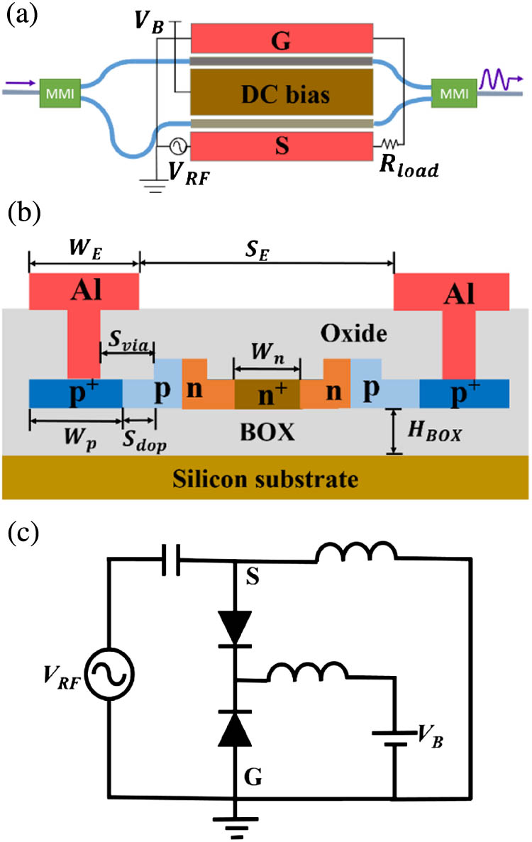
    Fig. 1. (a) Schematic structure of the BSPK modulator. (b) Cross section of modulation arms showing the single-drive TWE. (c) Equivalent circuit model of the TWE.
    Simulation results of MZI-1. (a) EE and EO S21 responses. (b) Z0 and neff versus RF frequency.
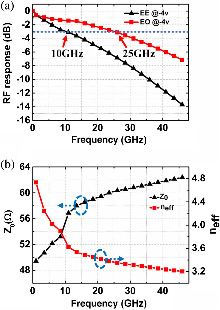
    Fig. 2. Simulation results of MZI-1. (a) EE and EO S21 responses. (b) Z0 and neff versus RF frequency.
    Effects of various TWE parameters: (a) WE, (b) SE, (c) Wn, (d) Wp, (e) Sdop, and (f) Svia on RF attenuation, Z0, and neff.
    Fig. 3. Effects of various TWE parameters: (a) WE, (b) SE, (c) Wn, (d) Wp, (e) Sdop, and (f) Svia on RF attenuation, Z0, and neff.
    Simulation results of MZI-2. (a) EE and EO S21 responses. (b) Z0 and neff versus RF frequency.
    Fig. 4. Simulation results of MZI-2. (a) EE and EO S21 responses. (b) Z0 and neff versus RF frequency.
    Measured optical transmission spectra under various bias voltages.
    Fig. 5. Measured optical transmission spectra under various bias voltages.
    Measured (a) S21 and (b) S11 responses of MZI-2 with DC bias voltage varying from 0 to −4 V.
    Fig. 6. Measured (a) S21 and (b) S11 responses of MZI-2 with DC bias voltage varying from 0 to 4V.
    (a) Measured BPSK signal eye diagram. (b) Measured BPSK constellation diagram. The signal data rate is 32 Gb/s.
    Fig. 7. (a) Measured BPSK signal eye diagram. (b) Measured BPSK constellation diagram. The signal data rate is 32 Gb/s.
    NameWE(μm)SE(μm)Wp(μm)Wn(μm)Svia(μm)Sdop(μm)
    MZI-1251620124.50.8
    MZI-2605020.716.216.70.5
    Table 1. TWE Parameters of BPSK Modulators
    Jinting Wang, Linjie Zhou, Haike Zhu, Rui Yang, Yanyang Zhou, Lei Liu, Tao Wang, Jianping Chen. Silicon high-speed binary phase-shift keying modulator with a single-drive push–pull high-speed traveling wave electrode[J]. Photonics Research, 2015, 3(3): 58
    Download Citation