Haiying Song, Shengwang Tan, Elshaimaa M. Emara, Yanjie Zhang, Shibing Liu*, Yao Li, and Haiyun Liu
Abstract
The effect of material surface morphology on the periodic subwavelength of nano-structures induced by a femtosecond (fs) laser was investigated systematically from the initial surface roughness, the different scratches, the pre-formed ripples, and the “layer-carving” technology experiments. The results of the comparative experiments indicate that the initial surface conditions of the target surface have no obvious effects on the spatial structured periods (SSPs) and the ripple orientation of the periodic nano-structures induced by a fs laser, which agreed well with the foretold present surface two-plasmon resonance (STPR) model. Furthermore, different shapes of nano-grids with high regularity and uniformity were obtained by fs-laser fabrication.Ultrafast laser–matter interactions in an extremely short temporal domain are of wide interest for both fundamental and applied research. As this field is a rapidly developed branch over the last decade, the unique properties of the characteristic nano-structures induced by a femtosecond (fs) pulse laser on solid surfaces have attracted much attention from correlative researchers due to the wide variety of applications in nano-optics[1–3], material physics[4,5], surface engineering[6–8], fabrication of electronic devices[9–11], etc. Thus, it is of great importance to understand the formation process of fs-laser-induced periodic subwavelength structures on solid surfaces, for the reason that it can enable us to control the structured patterns to reveal new aspects of their underlying peculiar functions[6,7]. In the formation mechanism, the various interpretations are proposed, such as the interference between a surface plasmon and incident laser[6,12,13], surface plasmon effects[14–16], initial surface roughness[17–19], kinds of heating[20], and resonant Mie scattering[21,22], which are intended to interpret the dynamic process of the periodic ripples induced by a fs laser. Many of the corresponding experiments about processing parameters were reported to discuss their effects on subwavelength formation, including the laser wavelength[23,24], the laser fluence[24–26], the pulse number[12,27] (or the laser scanning speed[23,28]), the polarization[26,29,30], the laser incident angle[30,31], and processing environments[10,32].
Recently, we proposed surface two-plasmon resonance (STPR) generated in the ultrafast interaction of a fs-laser pulse with surface plasmon produced on a target surface that gives birth to periodic subwavelength ripple structures[33]. The analytic formula regarding the spatial structured periods (SSPs) of the ripples was formulated, indicating that the SSPs of self-formed gratings strongly depend on the laser wavelength and the laser fluence. Also, some experiments about the corresponding processing parameters have been enacted, proving the veracity and effectiveness of the STPR model. Among these experiments, we found that the bi-direction scanning method (which is the back and forth scanning way) with some overlapped areas between the two scanning beams can make an aesthetically pleasing joint[23], so this draws interest to the research of the surface roughness effects on the induced periodic nano-structures. As for the actual engineering application, the devices’ surfaces cannot be very smooth or fine polished, so the surface morphology is an important factor for the nano-structures’ fabrication in the surface engineering field.
Some reports have described effects of the initial surface roughness on the surface ripples formation. Brueck et al.[34] first investigated the effects mechanism of the surface roughness; they inferred that the surface-plasma wave (SPW) is excited by surface-roughness-induced scattering from the incident field, and the growth of periodic ripple structures promoted by the spatial modulation of the optical intensity resulting from the interference between the incident wave and the SPW. Some experiments were also performed to discuss the problem, such as the effects of surface roughening to the fs-laser-induced ripples formation that were observed on single crystal 4H-SiC by Tomita et al.[17], and the results show that the coarse ripples formed are not affected by the initial roughness of irradiated materials, while the fine ripples are critically dependent on the surface roughness. They believed that the non-uniform photo-excited carrier distribution (or the non-uniform free electron density) due to the initial surface roughness plays a significant role for fine ripple formation. Another interesting experiment was done by Yang et al.[19], where the fs-laser-induced ripples on metal surfaces were formed by using a crossed two-step line-scribing method. The experiment results show that the ripple periodically tends to decrease with larger surface roughness but increase with higher laser fluence, and there exists a cut-off surface roughness value (which becomes smaller as the laser fluence increases) that prevents alteration of the ripple periodicity.
Sign up for Chinese Optics Letters TOC. Get the latest issue of Chinese Optics Letters delivered right to you!Sign up now
According to the above reports on the “STPR” ablation model and the “layer-carving” effects experiment, it is not difficult to find the effects of the surface morphology on the self-organizing formed periodic ripples within a limited range. Thus, in this Letter, we studied the differing effects of different material surface morphology on the periodic nano-ripples induced by a fs laser in order to achieve the micro/nano-structures on an actual device surface.
The laser used in this experiment is an amplified Ti:sapphire fs-laser system that generates 35 fs pulses of about 3.5 mJ/pulse at a 1 kHz repetition rate with a central wavelength of 800 nm. The tungsten (W) metal sample was placed in a three-dimensional (3D) mirco-moving stage. The horizontally polarized 800 nm fs laser was focused on the samples through an lens in a normal direction. The nano-structures were achieved by laser scanning through controlling the movement of the 3D stages. The experiments were performed in four contrast groups.
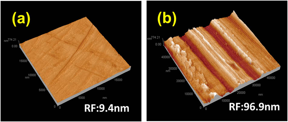
First, the two W samples that were polished and non-polished were prepared. Figure 1 shows the atomic force microscope (AFM) images of the sample surface, where the surface roughness was 9.4 nm and 96.9 nm respectively, and the two samples were scanned by a fs laser with fluence of at the scanning speed of 0.94 mm/s. Figure 2 shows the scanning electron microscope (SEM) pictures of the first contrast experiments. Figure 2(a) is the formed ripples on the polished sample surface, and Fig. 2(b) is the ripples formed on the non-polished sample surface. The ripple periods formed on the two samples were measured to ; they are almost the same. Anyway, the ripples’ surface morphology that formed on the non-polished sample has some little white spots due to the initial surface rough defects. These nano-particles should be the re-fusion of some remnant particles or the surface plasmas escape away from the material during the fs-laser process fabrication due to the rough surface. The results demonstrate that the initial roughness of the metal surface has no obvious effect on the periods and morphology of the formed ripples.

Figure 1.AFM images of the prepared W metals: (a) polished surface, (b) non-polished surface.
Figure 2.SEM pictures of periodic ripples induced by the fs laser on W metal surfaces: (a) polished, (b) non-polished.
Second, the initial scratches effects were studied. Some scratches were made deliberately on the polished sample; the ripples were obtained by the fs-laser-scanning method at fluence of . Figure 3 gives the observations by SEM, and, from the SEM pictures, we can see that the periodic nano-structures can still be obtained under different situations of surface defects, where the fs-laser pulse can handle these defects totally. For slight scratches with roughness of 30 nm like the SEM picture in Fig. 3(a), the scratches basically cannot affect the newly formed ripples, and also, the fs laser can repair the scratches to good looking ripples. For the scratches with the surface roughness of 100 nm like that in Figs. 3(b) and 3(c), the fs laser can avoid them and does not obstruct the processing work. For the deeper gully with depth of 600 nm, like the image in Fig. 3(d), the fs laser can stride over the gully easily, as well as there being no obstructions. The fs laser, just like a smart elf, can deal with minor obstructions that are encountered and obtain the nano-ripples with good looking morphology results. Anyway, the experiment results indeed provide us with some support for fabricating micro/nano-structures on the actual engineering application device surface.
Figure 3.SEM pictures of periodic ripples induced by a fs laser on a metal surface with defects.
Third, the ripples were induced by different scanning times in the same track, respectively, on the polished W metal surface. The fs-laser fluence used here was also with the scanning speed of 0.94 mm/s in six groups. Figure 4 shows the SEM pictures of the third contrast experiment results. The images are, respectively, one to six scanning times, following the formed ripples in the same track. The average periods of the ripples achieved were measured to 635, 633, 633, 630, 630, and 628 nm, respectively, where the ripple period reduces slightly as the number of scanning cycles increases.
Figure 4.SEM pictures of ripples achieved with different scanning times on the polished W surface: (a) one time, (b) two times, (c) three times, (d) four times, (e) five times, and (f) six times.
From the pictures, it can be seen that the main difference of the various scanning times is that some cracks occur in the ripple areas when the scanning times are five and six. While this again indicates that the pre-formed ripples will not have a significant effect on the later fabrication of ripples, the obvious change is the ablation depth. Figure 5 shows the change curve of the ripple depth measured by AFM, and the depth increases every time. The curve changes gradually from steep to gentle; this is due to the depth of the ripple valley being a little far away from the focus spot of the fs-Gaussian pulse, and the laser pulse does not have enough power to ablate the materials to such a high depth.
Figure 5.Curve of ripple depth changes with scanning times.
The above experiments again present a good verification of the STPR mechanism that an analogous surface carving arises from phase-locked STPR wave patterns, and the periodic structures induced by a fs laser based on the STPR ablation remain relatively independent on the respective temporal and spatial areas and coalesce in the overlapped area. Thus, according to the STPR model and the “layer-carving” notion, we carried out nano-structuring experiments by using a two-beam multi-irradiating scanning W target surface in the designed double optical path exposure delay system, as illustrated in Fig. 6. The sample surface was simply polished mechanically with surface roughness of 10 nm to avoid too high reflectivity, and the pulse profile was properly shaped by a Focal- Shaper 9 system. A linear polarized normal incident fs laser beam is split into two equal beams by a non-polarizing 50/50 beam splitter, denoted as and ; the delay time between these two beams is tuned by a motorized time-delay-line (TDL), which is used to adjust the times of the two beams (pulses) arriving coaxially at the same position of the target surface, and, thus, the same location of the surface can be exposed to these two time-delayed and focused laser beams asynchronously. To examine the influence of these two exposures asynchronously on the surface structures at the same location, a polarizing prism (PP) is used to alter the polarization directions between () and (), as shown in Fig. 6, so as to form a certain cross angle between the electric fields ( and ) of laser beams. The laser fluence of each beam road used here was .
Figure 6.Overview of the experimental setup for nano-structures experiments using two beams with crossed light polarizations. BS is non-polarizing 50/50 beam splitter, PP is polarizing prism, Re is reflecting mirror, and TDL is a motorized time-delay-line.
Figure 7 gives the SEM images of large nano-grids by the nano-structures scanning system, where the pictures present the good looking nano-structures. Figure 7(a) is the SEM image of square lattices with the structure size of , which were obtained by the orthogonal laser field and . Figure 7(b) is the SEM image of parallelogram grids, which were obtained under the situation that the polarization directions of the laser fields and show a 45° angle. The experiment results clearly illustrate that the initial surface condition does not affect the later nano-structures induced by the fs laser, and the ripples still remain independent periods and orientations. The nano-grids experiments further verify the prediction of fabricating complex geometric configurations based on the STPR “layer-carving” effect; this will establish a good basis of micro/nano-structures controllable fabrication, according to engineering expectations.
Figure 7.SEM images of nano-gratings produced by pulses with different crossed angles: (a) the electric field and is orthogonal, (b) the angle between and is 45°. The period of the gratings is about 610–630 nm.
In conclusion, the effects of material surface morphology on the periodic subwavelength patterns induced by a fs laser were investigated systematically from the comparative experiments of four groups. The results indicate that the initial surface morphology on the target surface has no obvious effects on the periodic nano-structures formation, the SSP, and the ripples’ orientation induced by the fs-laser process, which again satisfactorily verified the present STPR model. In morphology, the nano-grids in the “layer-carving” experiment improve the aesthetic quality with a high regularity and uniformity. All the verification tests in this Letter would provide us with a good method to realize unique surface functions on complex surfaces of actual micro-devices.
References
[1] S. Juodkazis, V. Mizeikis, H. Misawa. J. Appl. Phys., 106, 051101(2009).
[2] F. Chen, J. R. Vázquez de Aldana. Laser Photon. Rev., 8, 251(2014).
[3] A. Pan, T. Chen, C. Li, X. Hou. Chin. Opt. Lett., 14, 052201(2016).
[4] W. T. Chen, M. L. Tseng, C. Y. Liao, P. C. Wu, S. Sun, Y. W. Huang, C. M. Chang, C. H. Lu, L. Zhou, D. W. Huang, A. Q. Liu, D. P. Tsai. Opt. Express, 21, 618(2013).
[5] M. L. Tseng, Y.-W. Huang, M.-K. Hsiao, H. W. Huang, H. M. Chen, Y. L. Chen, C. H. Chu, N.-N. Chu, Y. J. He, C. M. Chang, W. C. Lin, D.-W. Huang, H.-P. Chiang, R.-S. Liu, G. Sun, D. P. Tsai. ACS Nano, 6, 5190(2012).
[6] A. Y. Vorobyev, C. Guo. Laser Photon. Rev., 7, 385(2013).
[7] R. Buividas, M. Mikutis, S. Juodkazis. Prog. Quantum Electron., 38, 119(2014).
[8] A. Y. Vorobyev, C. Guo. J. Appl. Phys., 117, 033103(2015).
[9] M. L. Tseng, C. M. Chang, B. H. Chen, Y.-W. Huang, C. H. Chu, K. S. Chung, Y. J. Liu, H. G. Tsai, N.-N. Chu, D.-W. Huang, H.-P. Chiang, D. P. Tsai. Nanotechnology, 23, 444013(2012).
[10] J. Meng, H. Y. Song, X. Li, S. B. Liu. Appl. Phys. A, 118, 1197(2015).
[11] A. Y. Vorobyev, V. S. Makin, C. Guo. Phys. Rev. Lett., 102, 234301(2009).
[12] M. Huang, F. Zhao, Y. Cheng, N. Xu, Z. Xu. ACS Nano, 3, 4062(2009).
[13] Y. Huang, S. Liu, W. Li, Y. Liu, W. Yang. Opt. Express, 17, 20756(2009).
[14] F. Garrelie, J. P. Colombier, F. Pigeon, S. Tonchev, N. Faure, M. Bounhalli, S. Reynaud, O. Parriaux. Opt. Express, 19, 9035(2011).
[15] J. Bonse, A. Rosenfeld, J. Kruger. J. Appl. Phys., 106, 104910(2009).
[16] D. Kim, W. Jang, T. Kim, A. Moon, K. S. Lim, M. Lee, I. B. Sohn, S. Jeong. J. Appl. Phys., 111, 093518(2012).
[17] T. Tomita, K. Kinoshita, S. Matsuo, S. Hashimoto. Appl. Phys. Lett., 90, 153115(2007).
[18] J. E. Sipe, J. F. Young, J. S. Preston, H. M. van Driel. Phys. Rev. B, 27, 1141(1983).
[19] Y. Yang, J. Yang, L. Xue, Y. Guo. Appl. Phys. Lett., 97, 141101(2010).
[20] T. Y. Hwang, C. L. Guo. J. Appl. Phys., 109, 083521(2011).
[21] Y. Tanaka, G. Obara, A. Zenidaka, N. N. Nedyalkov, M. Terakawa, M. Obara. Opt. Express, 18, 27226(2010).
[22] G. Obara, N. Maeda, T. Miyanishi, M. Terakawa, N. N. Nedyalkov, M. Obara. Opt. Express, 19, 19093(2011).
[23] H. Y. Song, Y. J. Zhang, X. M. Dong, S. B. Liu. Chin. Opt. Lett., 14, 123202(2016).
[24] M. Hashida, Y. Ikuta, Y. Miyasaka, S. Tokita, S. Sakabe. Appl. Phys. Lett., 102, 174106(2013).
[25] K. M. T. Ahmmed, C. Grambow, A. Kietzig. Micromachines, 5, 1219(2014).
[26] K. Zhou, X. Jia, H. Xi, J. Liu, D. Feng, S. Zhang, Z. R. Sun, T. Q. Jia. Chin. Opt. Lett., 15, 022201(2017).
[27] A. Y. Vorobyev, V. S. Makin, C. Guo. J. Appl. Phys., 101, 034903(2007).
[28] J. W. Yao, C. Y. Zhang, H. Y. Liu, Q. F. Dai, L. J. Wu, S. Lan, A. V. Gopal, V. A. Trofimov, T. M. Lysak. Opt. Express, 20, 905(2012).
[29] B. K. Nayak, M. C. Gupta. Opt. Lasers Eng., 48, 966(2010).
[30] X. M. Dong, H. Y. Song, S. B. Liu. Chin. Opt. Lett., 13, 071001(2015).
[31] Q. Z. Zhao, S. Malzer, L. J. Wang. Opt. Lett., 32, 1932(2007).
[32] T. Her, R. J. Finlay, C. Wu, S. Deliwala, E. Mazur. Appl. Phys. Lett., 73, 1673(1998).
[33] H. Y. Song, S. B. Liu, H. Y. Liu, Y. Wang, T. Chen, X. M. Dong. Opt. Express, 24, 12151(2016).
[34] S. R. J. Brueck, D. J. Ehrlich. Phy. Rev. Lett., 48, 1678(1982).