State Key Laboratory of Advanced Optical Communication Systems and Networks, Intelligent Microwave Lightwave Integration Innovation Center (iMLic), Department of Electronic Engineering, Shanghai Jiao Tong University, Shanghai 200240, China
Kangjia Zheng, Weiwen Zou, Lei Yu, Na Qian, Jianping Chen, "Stability optimization of channel-interleaved photonic analog-to-digital converter by extracting of dual-output photonic demultiplexing," Chin. Opt. Lett. 18, 012502 (2020)
Copy Citation Text
We investigate a channel-interleaved photonic analog-to-digital conversion (PADC) system’s ability to work stably over a long duration with an optimal driving voltage. The influence of optimum bias point drift of a Mach–Zehnder modulator (MZM)-based photonic switch on this system was analyzed theoretically and experimentally. The feasibility of extracting feedback signals from the PADC system was derived. A high-stability channel-interleaved PADC was constructed by extracting a feedback signal from a parallel demultiplexing module to control the MZM-based photonic switch’s driving voltage. Consequently, the amplitude mismatch between the channels was limited to within 0.3 dB over 12 hours of operation.
In recent years, many advances have been made in photonic analog-to-digital conversion (PADC) technology to overcome the performance bottleneck in traditional electronic analog-to-digital conversion technology[1–6]. The PADC system consists of a photonic front-end and an electronic back-end to combine the high performance of photonic technology with the convenience of electronic technology, thereby providing an ideal solution of signal reception processing for next-generation radar and communication[7–12]. Recent research has been investigated to develop the PADC systems, including system architecture innovation, device performance optimization, and signal processing algorithm improvements[3,4,13,14].
However, both radar and communication systems need to be able to work stably for long periods of time. Their operating environments are complex, and environmental factors such as temperature, humidity, and pressure can change significantly during operation. These will lead to an optimal bias point drift of the Mach–Zehnder modulator (MZM)[15,16], a vital component in the PADC system that serves as a sampling gate and photonic switch[4,17]. This drift will degrade the high-precision characteristics of the PADC system. To maintain stable operating conditions of the PADC system in practice, optimum bias point selection and controlling technologies should be studied. Although mature automatic bias control (MBC) devices are currently available, their application will undoubtedly increase the size and weight of PADC systems, especially those of 4- or 8-channel PADC systems with cascaded MZMs[3]. This is contrary to the trend of miniaturizing and integrating modern radar and communication systems[18].
In this Letter, we investigate the characteristics of demultiplexed signals in a channel-interleaved PADC system. The influence of optimum bias point drift of an MZM-based photonic switch on the channel-interleaved PADC system is analyzed theoretically and experimentally. Simultaneously with demultiplexing, the offset of the optimum bias voltage of the MZM-based photonic switch is extracted through system sampling and provided as a feedback signal to the system to change the driving voltage applied to the photonic switch. In long-term experiments, the bias-point-drift-induced fluctuation of the PADC system is suppressed from 3.4 dB to 0.3 dB.
Sign up for Chinese Optics Letters TOC. Get the latest issue of Chinese Optics Letters delivered right to you!Sign up now
The switching response of an MZM-based photonic switch can be expressed as[4]
Therefore, the time-domain expression of the two demultiplexed channels can be given as where is the maximum transmittance of the MZM-based photonic switch. is the extinction ratio of the photonic switch, where is the minimum transmittance of the MZM-based photonic switch. is the time-domain expression of the driving signal. and are the amplitude and frequency of the driving signal, respectively. is the phase offset between the sampling pulse and the driving signal. is the half-wave voltage of the MZM(RF), and is the half-wave voltage of the MZM(DC). is the driving voltage applied to the MZM-based photonic switch. , where is the shape of the optical pulse, is the temporal interval of the sampling series, and is the time-domain expression of the sampled signal.
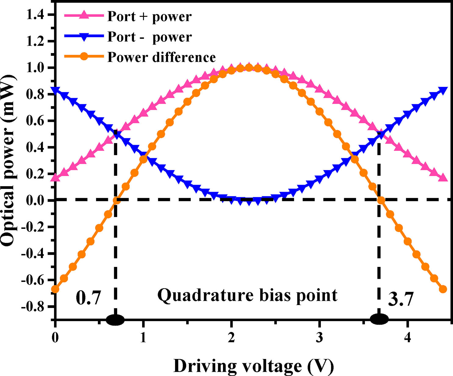
Equation (2) shows that there is a fixed offset between the two signals after demultiplexing, implying that they have a complementary relationship in signal power. A numerical simulation based on Eqs. (1) and (2) is implemented to intuitively identify the relationship between the power of two output optical signals after demultiplexing under different working points; the normalized result is shown in Fig. 1. The system sampling rate is set to 20 GS/s. The maximum transmittance is and the extinction ratio is . The driving signal amplitude is and the driving signal frequency is . The half-wave voltage of the MZM(DC) is . The quadrature bias point is set to be 0.7 V and 3.7 V. The sampled signal is a 2.4 GHz single-tone signal with 20 dBm power. After demultiplexing, these two optical signals have an obvious complementary relationship in signal power. These two optical pulse trains have the same optical power only when the driving voltage applied to the MZM-based photonic switch is equal to the quadrature bias voltage.
Figure 1.Simulation results of the relationship between the powers of two output optical signals after demultiplexing under different working points.
Furthermore, we can substitute and to simplify Eq. (2) because a previous study found that the PADC system has a relatively high efficiency under these settings[4]. Therefore, the frequency-domain expression of the two demultiplexed channels can be given as where is the effective amplitude of the sampled signal; is the frequency of the sampled signal; is the Fourier transform of ; is the system sampling rate before demultiplexing; and , , and can be expressed as follows:
According to Eqs. (3) and (4), one can find that the bias point drift of the MZM-based photonic switch results in an amplitude mismatch between the two signals after demultiplexing when the sampled signal falls into the Nyquist interval; in this case, because and have opposite trends when changes. Note that the Nyquist interval corresponds to the sampling rate of each demultiplexed channel, which is half before demultiplexing. When the sampled signal falls outside the Nyquist interval, the bias point drift of the MZM-based photonic switch results in the response efficiencies of both channels declining by the same amount after demultiplexing because the response efficiencies of both channels are determined by .
The effect of bias point drift of the MZM-based photonic switch in the PADC system is experimentally investigated based on the classic architecture, a schematic of which is shown in Fig. 2. An actively mode-locked laser (AMLL; Calmar PSL-10-TT) is used to generate the optical sampling pulse train. A 20 GHz microwave signal generated by a low-noise microwave generator (Keysight E8257D) is used to provide a seed signal to the AMLL. The optical sampling pulse train is amplified by an optical amplifier (AMP; Calmar AMP-ST30) and passes through an MZM (MZM1, Photoline MXIQLN-40) with 40 GHz input bandwidth. The microwave generator (N5083B) is used to generate the signal to be sampled. A microwave generator (SMA100B) is used to generate a 10 GHz driving signal. The dual-output MZM (MZM2, EOSpace AX-1x2-0MSS-20) is used as a photonic switch driven by the 10 GHz driving signal. The sampled optical signal is demultiplexed into two channels by the photonic switch. The demultiplexed signals are photoelectrically converted by two 10 GHz bandwidth PDs (Conquer PDA-10 G-InGaAs-SM-FA) and digitized by two channels of a real-time oscilloscope (Keysight MSO804A). In addition, the low-noise microwave source (Keysight E8257D) that provides the seed signal to the laser outputs a 10 MHz reference signal to the microwave generator (SMA100B) and the oscilloscope as a reference clock.
Figure 2.Experimental setup of a high-stability channel-interleaved PADC system with a feedback link. AMLL, actively mode-locked laser; AMP, optical amplifier; MZM, Mach–Zehnder modulator; TDL, time delay line; PD, photodiode; ADC, analog-to-digital converter; OC, optical coupler; BPD, balanced photodiode; DSP, digital signal processor; PPS, programmable power supply.
Two single-tone signals with frequencies of 2.4 GHz and 12.4 GHz are applied to the sampling gate, respectively. As in the theoretical derivation, the fiber delay line is adjusted until the phase offset between the sampling pulse and the driving signal is 0, and the amplitude of the driving signal is adjusted until is satisfied. The sampling rate of the PADC system is . Figure 3 shows the experimental results. When the sampled RF signal has a frequency of 2.4 GHz, a significant amplitude mismatch is seen between the two signals after demultiplexing when deviates from (quadrature bias point). When , there is no switching response. Only when , there is no amplitude mismatch between the two signals after demultiplexing. Previous studies have shown that amplitude mismatch reduces the effective number of bits (ENOB) of a PADC system[19]. When the sampled RF signal has frequency of 12.4 GHz, the digitized spectrum of the 12.4 GHz sampled signal is folded to 2.4 GHz according to the subsampling principle[20]. Although no obvious amplitude mismatch is seen between the two signals after demultiplexing when deviates from , the response efficiencies of both channels declined by the same amount after demultiplexing. The larger the offset, the lower is the response efficiency. This is consistent with the results derived using Eqs. (3) and (4). This phenomenon also undoubtedly reduces the ENOB of the PADC system. Regardless of the sampled signal frequency, the bias point drift of the MZM-based photonic switch degrades the ENOB of the PADC system. Therefore, the experimental results are completely consistent with the theoretical derivation results.
Figure 3.Experimental results of the relationship between demultiplexing performance and driving voltage in the PADC system when the frequency of the input signal to be sampled is (a) 2.4 GHz and (b) 12.4 GHz.
Previous experiments often overlooked the bias point drift of the MZM. However, this factor cannot be avoided during long-term operation. This effect is more pronounced in multistage multichannel PADC systems (e.g., those with 4 or 8 channels). Therefore, varying the driving voltage with the optimum bias point drift of the MZM is an important way to further improve the ability of PADC systems to work stably for a long duration. Furthermore, considering the integration trend of PADC systems, a feedback link should be constructed based on the system characteristics.
Figure 2 further shows the schematic of high-stability channel-interleaved PADC systems with automatically selected driving voltages. Inspired by the power characteristics of the two optical signals after demultiplexing, 10% optical signals of both demultiplexed signals are divided using the two 90:10 optical couplers, which serve as feedback signals. In the feedback link, the two feedback optical signals are converted into feedback voltage values by a narrow-bandwidth balanced photodiode (BPD, DC-300 MHz) whose output signal includes a DC component. Based on the working principle of the photodiode (PD), the value of the DC output component depends on the input optical power and the responsiveness of the PD. The optical pulse in the parallel demultiplexing module has a high frequency that is not within the frequency response of the PD; therefore, the final output of the PD is only the DC component. Considering that the response characteristics of the two PDs in the BPD are approximately identical, the BPD output can be considered as the result of power comparison of the two optical signals after demultiplexing. The feedback voltage value is read by a digitizer and passed to the processor. According to the feedback voltage value, the processor changes the driving voltage provided by the programmable power supply (PPS) to the photonic switch. This feedback is used to control the photonic switch (MZM2) of the channel-interleaved PADC system. Note that the response rate of the feedback subsystem depends on the response rate of the digital signal processor and the programmable power supply, which is much faster than the optimum bias point drift rate of the system. It is an automatic control system for real-time feedback that does not affect the operation of the PADC system.
To verify the validity of the feedback signal, a step-increasing driving voltage is applied to the photonic switch of MZM2 and the feedback signal value is measured in real time. In addition, the photonic switch transmission curve is measured immediately thereafter. Figure 4 shows the experimental results; they are consistent with the theoretical ones. When the BPD output is 0 V, the photonic switch is exactly at the optimal working point. Therefore, the driving voltage can be changed accurately according to the magnitude of the feedback value to ensure that the photonic switch works at the optimal working point. It is worth noting that this feedback architecture is also applicable when the dual-output modulator serves as the sampling gate.
Figure 4.Experimental results of the relationship between the feedback signal and transmission function of the photonic switch (MZM2).
A long-term comparative test of the two experimental architectures with and without the feedback optimization is conducted. A 2.4 GHz signal with 10 dBm power is input to the PADC system. As analyzed previously, the two-channel 2.4 GHz input signal shows an amplitude mismatch after demultiplexing owing to bias point drift of the MZM-based photonic switch. Further, the larger the drift, the more serious is the amplitude mismatch. Therefore, a spectrum analyzer (FSW43) is used to detect the amplitudes of the 2.4 GHz signals in the two channels and compare their differences. The optimized PADC system could work very stably over a long duration [see Fig. 5(b)], and its amplitude mismatch varies within 0.3 dB around the fixed difference. In contrast, the classic architecture fluctuates more than 3.4 dB over only 12 hours of operation and this seriously affects the high-precision characteristics of the system [see Fig. 5(a)].
Figure 5.(a) Measured result of the amplitude mismatch between channels after demultiplexing in a channel-interleaved PADC system without a feedback link. (b) Measured result of the amplitude mismatch between channels after demultiplexing in a channel-interleaved PADC system with the feedback optimization.
In conclusion, we have theoretically and experimentally verified that the bias point drift of MZM-based photonic switches deteriorates the performance of PADC systems. Therefore, we have optimized a PADC system to perform real-time monitoring feedback and theoretically and experimentally verified the rationality of using the feedback signal. Finally, we conducted a long-term comparison test between the two experimental architectures with and without the feedback optimization and found that the optimized PADC system architecture has an excellent ability to work stably over a long duration: the bias-point-drift-induced fluctuation of the PADC system is suppressed from 3.4 dB to 0.3 dB in the long-term test. In the next study, we are planning to adopt the feedback optimization to a multiple-channel PADC system.
Kangjia Zheng, Weiwen Zou, Lei Yu, Na Qian, Jianping Chen, "Stability optimization of channel-interleaved photonic analog-to-digital converter by extracting of dual-output photonic demultiplexing," Chin. Opt. Lett. 18, 012502 (2020)