• Opto-Electronic Science
  • Vol. 2, Issue 12, 230017 (2023)
Baiheng Zhao1, Junwei Cheng1, Bo Wu1, Dingshan Gao1, Hailong Zhou1, and Jianji Dong1、2、*
Author Affiliations
  • 1Wuhan National Laboratory for Optoelectronics, Huazhong University of Science and Technology, Wuhan 430074, China
  • 2Optics Valley Laboratory, Wuhan 430074, China
  • show less
    DOI: 10.29026/oes.2023.230017 Cite this Article
    Baiheng Zhao, Junwei Cheng, Bo Wu, Dingshan Gao, Hailong Zhou, Jianji Dong. Integrated photonic convolution acceleration core for wearable devices[J]. Opto-Electronic Science, 2023, 2(12): 230017 Copy Citation Text show less
    Schematic of a computing system based on the integrated convolution acceleration core (PCAC) chip.
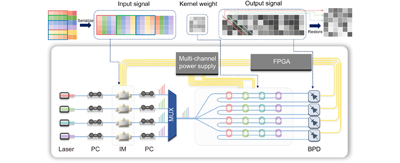
    Fig. 1. Schematic of a computing system based on the integrated convolution acceleration core (PCAC) chip.
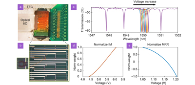
    (a) Detailed photos of the packaged layout chip show the MRR array in the center, with the photonics chip on the right combined with the leads of the customized printed circuit board (PCB) for computation and control. On the left, there is an optical input/output port using a fiber V-groove, and the entire assembly is mounted on a TEC for heat dissipation. (b) The micrograph of the MRR array and detailed photo of a single MRR. (c) The transmission spectra of the MRR array. Different voltages (800–1800 mV, 100 mV/step) are applied to the third MRR. Similar results can be obtained when the voltage is applied to other MRRs. (d) The transmission rate of a single IM on the chip under voltage tuning. These curves represent the normalized W-V mapping. (e) The transmission rate of a single MRR on the chip under voltage tuning. These curves represent the normalized W-V mapping.
    Fig. 2. (a) Detailed photos of the packaged layout chip show the MRR array in the center, with the photonics chip on the right combined with the leads of the customized printed circuit board (PCB) for computation and control. On the left, there is an optical input/output port using a fiber V-groove, and the entire assembly is mounted on a TEC for heat dissipation. (b) The micrograph of the MRR array and detailed photo of a single MRR. (c) The transmission spectra of the MRR array. Different voltages (800–1800 mV, 100 mV/step) are applied to the third MRR. Similar results can be obtained when the voltage is applied to other MRRs. (d) The transmission rate of a single IM on the chip under voltage tuning. These curves represent the normalized W-V mapping. (e) The transmission rate of a single MRR on the chip under voltage tuning. These curves represent the normalized W-V mapping.
    (a) Experimental setup of the PCAC chip for performing convolutional operations. (b) Original image used for demonstrating the convolution effect. (c) Convolution kernels used: Bottom sobel, Top sobel, Left sobel. (d) Corresponding convolution image results.
    Fig. 3. (a) Experimental setup of the PCAC chip for performing convolutional operations. (b) Original image used for demonstrating the convolution effect. (c) Convolution kernels used: Bottom sobel, Top sobel, Left sobel. (d) Corresponding convolution image results.
    (a) Schematic diagram of the convolutional neural network (CNN) architecture suitable for first-person digit gesture recognition with depth information. (b) Probability of recognition for the 10 gestures after performing the convolutional layer computation using the PCAC chip as a replacement for the computer.
    Fig. 4. (a) Schematic diagram of the convolutional neural network (CNN) architecture suitable for first-person digit gesture recognition with depth information. (b) Probability of recognition for the 10 gestures after performing the convolutional layer computation using the PCAC chip as a replacement for the computer.
    (a) Scatter plot comparing measured results with calculated results for Gesture 2. (b) Probability distribution of the error offset in the experimental results, resembling a Gaussian curve. (c) Offset of each point during the computation process. (d) Results of the first layer convolution computation obtained through electronic computation. (e) Results of the first layer convolution computation obtained through optical-electronic computation using the PCAC chip.
    Fig. 5. (a) Scatter plot comparing measured results with calculated results for Gesture 2. (b) Probability distribution of the error offset in the experimental results, resembling a Gaussian curve. (c) Offset of each point during the computation process. (d) Results of the first layer convolution computation obtained through electronic computation. (e) Results of the first layer convolution computation obtained through optical-electronic computation using the PCAC chip.
    ComponentsVoltage(V)Current(A)Power(W)
    Lasers~10×10-3×4=0.04
    On ring heatersV¯2~5×10⁻³~0.01×16=0.16
    Intensity modulator1V¯70.2661.862
    Intensity modulator2V¯6.50.2781.807
    Intensity modulator3V¯70.2721.904
    Intensity modulator4V¯7.50.2591.943
    System’s power consumption7.716
    TEC for PCAC chip6.1450.533.257
    CPU~30
    Total power consumption40.973
    Table 1. Estimated power consumption of the proof-of-concept system.
    Baiheng Zhao, Junwei Cheng, Bo Wu, Dingshan Gao, Hailong Zhou, Jianji Dong. Integrated photonic convolution acceleration core for wearable devices[J]. Opto-Electronic Science, 2023, 2(12): 230017
    Download Citation