Shen Xu, Hongyang Zhu, Lijun Zhang, Yanan Yue, Xinwei Wang. Exploration of Physical Mechanism in Laser Assisted Near-field Nanomanufacturing[J]. Chinese Journal of Lasers, 2021, 48(6): 0600001
Search by keywords or author
- Chinese Journal of Lasers
- Vol. 48, Issue 6, 0600001 (2021)
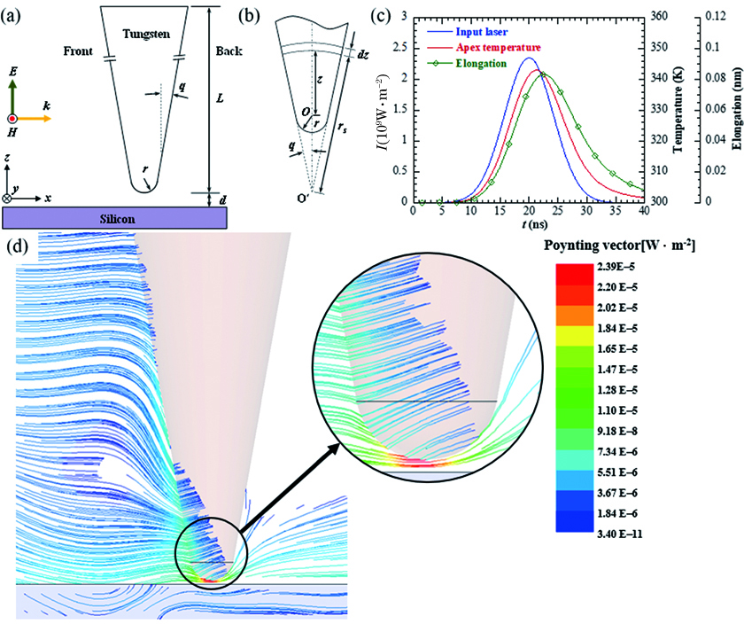
![Simulation of near field optical, thermal, and stress fields of the tip under laser irradiation[8]. (a) Configuration of the tip-substrate system under modeling; (b) geometric configuration of the tip;(c) evolution of the laser intensity, apex temperature, and elongation (thermal expansion) with time; (d) Poynting vector distribution around the tip](/richHtml/zgjg/2021/48/6/0600001/img_1.jpg)
Fig. 1. Simulation of near field optical, thermal, and stress fields of the tip under laser irradiation[8]. (a) Configuration of the tip-substrate system under modeling; (b) geometric configuration of the tip;(c) evolution of the laser intensity, apex temperature, and elongation (thermal expansion) with time; (d) Poynting vector distribution around the tip
![Microscale spatially resolved thermal response of Si tip to laser irradiation[9]. (a) SEM image of the front plane of the AFM silicon tip; (b) SEM image of the side plane of the AFM silicon; (c) positional relationship between the laser beam at the focal spot and the tip when the laser illuminates the tip side; (d) the moving directions of laser spot with respect to the tip during the experiment; (e) Raman shift, temperature, and Raman intensity v](/richHtml/zgjg/2021/48/6/0600001/img_2.jpg)
Fig. 2. Microscale spatially resolved thermal response of Si tip to laser irradiation[9]. (a) SEM image of the front plane of the AFM silicon tip; (b) SEM image of the side plane of the AFM silicon; (c) positional relationship between the laser beam at the focal spot and the tip when the laser illuminates the tip side; (d) the moving directions of laser spot with respect to the tip during the experiment; (e) Raman shift, temperature, and Raman intensity v
Fig. 3. Noncontact temperature measurement in near-field laser heating[11]. (a) Schematic of experimental setup for thermal probing using the apertureless NSOM; (b) relationship between the measured silicon surface temperature and laser spot position on the tip (a weak laser scattering intensity in the x axis indicates the laser spot is on tip apex, while a strong scattering intensity indicates the laser spot is on the upper part of the tip near t
Fig. 4. Simulation of near-field optical field in silicon tip[11].(a) Tip-substrate domain in the simulation; (b) front view of the electric field around the tip distributed in the y=0 plane; (c) top view and cross-sectional view of the electric field around the tip under the tip apex; (d)electric field distribution in the A-A' plane; (e) electric field distribution in the cross-section; (f) schematic of the thermal resistance calculation o
Fig. 5. Nanoscale mapping of physics fields under 1210 nm silica micro-particles assisted near-field heating[14]. (a) Under different laser irradiation energy, the variation of Raman intensity I along the mapping direction; (b) variations of Raman intensity I, Raman shift ω, and linewidth Γ of silicon in the x direction with laser intensity of 3.1×10⁹ W/m2; (c) deviation between the laser beam axis
Fig. 6. Spatial resolution limit of silica microsphere assisted near-field detection[14].(a) Trend of Imax/Imin against the diameter of the silica particle; (b) variation of Raman intensity I along the x direction for a silicon wafer under a 200 nm diameter silica particle
Fig. 7. Simulation and error analysis of electric and temperature fields in silica particles and the silicon substrate[14]. (a) Modeling results of the electric field for two situations: laser spot on a single particle and between two particles; (b) under the near-field focused laser heating, silicon wafer temperature variation along the thickness (z) direction directly under a 1210 nm silica particle, and the inset shows the temperature distribut
Fig. 8. Optical field, temperature field, and thermal stress field at the surface and in cross-section of the silicon substrate[15]. (a) Optical field; (b) temperature field; (c) thermal stress field introduced by the temperature rise
Fig. 9. Schematics of MD model and laser beam absorption in the material[19]. (a) Schematic of MD model; (b) schematic of laser beam absorption in the material
Fig. 10. Temperature distribution and evolution in x-z cross-section[19]
Fig. 11. Normal stress σrr(MPa) development and propagation in x-y plane[19]
Fig. 12. Snapshots of argon atom positions in x-z cross-section at different moments[19]
Fig. 13. Solidification and epitaxial regrowth in surface nanostructuring[20]. (a) Snapshots of argon atom positions in x-z cross-section during a long time solidification; (b) magnification in the x-z cross-section at t=2 ns to show the epitaxial growth and atomic dislocation
Fig. 14. Distribution of function Φ(ri,z) at different times in x-z cross-section[20]
Fig. 15. Effects of laser fluence on solidification of melts[21]. (a) Evolution of thickness and lowest melting position of the molten material with time; (b) final surface profiles under different laser pulse energies after complete solidification
Fig. 16. Physical properties distribution in a cross-section of the system at 200 ps[24]. (a) Density (nm-3); (b) temperature (K); (c) pressure (MPa)
Fig. 17. Evolution of shock wave front temperature, position and Mach number with time[24]
Fig. 18. Evolution of atom positions during shock wave formation and propagation for different cases (β=Mgas/Msolid, λ=pambient/pref) at different instants[25] (red dots: target atoms; blue dots: ambient gas atoms)
|
Table 1. Detailed information about the three computational domains studied in Ref.[21]

Set citation alerts for the article
Please enter your email address


