• Photonics Research
  • Vol. 4, Issue 3, 0106 (2016)
Markus Sieger and Boris Mizaikoff*
Author Affiliations
  • Institute of Analytical and Bioanalytical Chemistry, Ulm University, Albert-Einstein-Allee 11, 89081 Ulm, Germany
  • show less
    DOI: 10.1364/prj.4.000106 Cite this Article Set citation alerts
    Markus Sieger, Boris Mizaikoff. Optimizing the design of GaAs/AlGaAs thin-film waveguides for integrated mid-infrared sensors[J]. Photonics Research, 2016, 4(3): 0106 Copy Citation Text show less
    Cross section of the simulation model (50 μm×50 μm) comprising a GaAs/AlGaAs waveguide with a 6 μm AlGaAs layer (optical buffer), a 6 μm GaAs layer (actual waveguide), and a 20 μm thick GaAs substrate. The width (w), the thickness of the absorbed layer (dl) simulating an analyte, and the refractive index of the outer medium (no) were varied during the simulations.
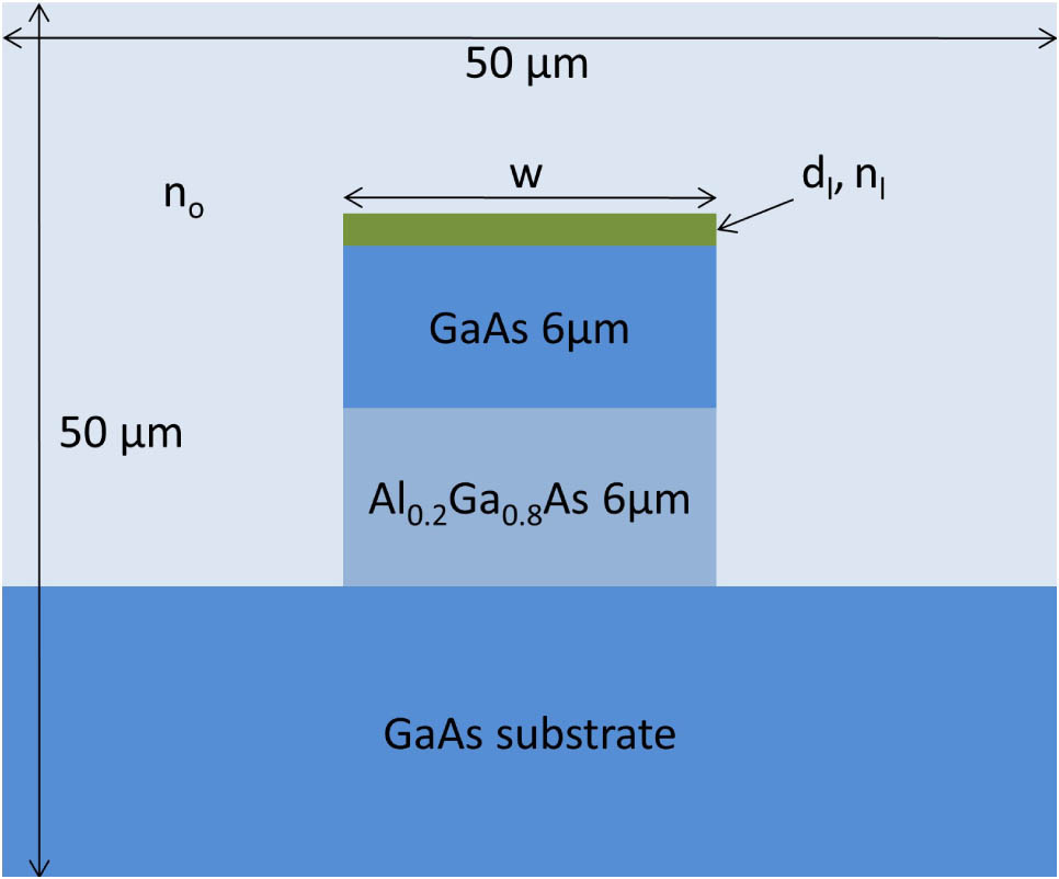
    Fig. 1. Cross section of the simulation model (50  μm×50  μm) comprising a GaAs/AlGaAs waveguide with a 6 μm AlGaAs layer (optical buffer), a 6 μm GaAs layer (actual waveguide), and a 20 μm thick GaAs substrate. The width (w), the thickness of the absorbed layer (dl) simulating an analyte, and the refractive index of the outer medium (no) were varied during the simulations.
    Dependence of the modal behavior on the width of the waveguide (A) for the amide region (1800–1600 cm−1), and (B) for the carbohydrate region (1200–1000 cm−1). (C) The fundamental guided TM00 mode of a 5 μm wide waveguide, and (D) the first-order TM01 mode of a 11 μm wide waveguide at a wavelength at 1700 cm−1 are also illustrated.
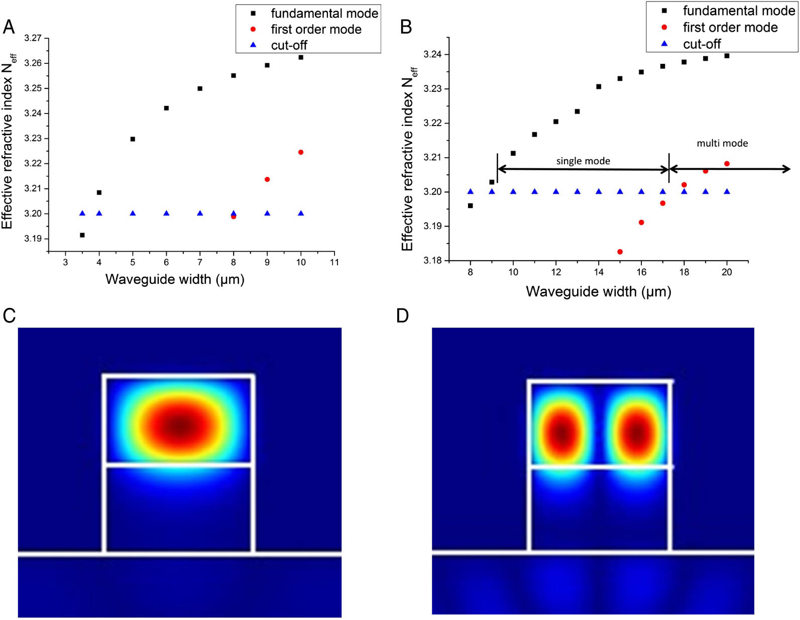
    Fig. 2. Dependence of the modal behavior on the width of the waveguide (A) for the amide region (18001600  cm1), and (B) for the carbohydrate region (12001000  cm1). (C) The fundamental guided TM00 mode of a 5 μm wide waveguide, and (D) the first-order TM01 mode of a 11 μm wide waveguide at a wavelength at 1700  cm1 are also illustrated.
    Exponential fit of the effective refractive index of a 13 μm wide waveguide at a wavelength at 1100 cm−1 as a function of the absorbing analyte layer thickness.
    Fig. 3. Exponential fit of the effective refractive index of a 13 μm wide waveguide at a wavelength at 1100  cm1 as a function of the absorbing analyte layer thickness.
    Linear fit of the effective refractive index of a 5 μm wide waveguide at a wavelength at 1700 cm−1 as a function of the refractive index of the outer medium.
    Fig. 4. Linear fit of the effective refractive index of a 5 μm wide waveguide at a wavelength at 1700  cm1 as a function of the refractive index of the outer medium.
    (Top) Normalized electric field component along the center axis of a waveguide versus the waveguide width. Inset illustrates the waveguide section of the simulated electric field for a 5 μm wide waveguide at 1700 cm−1. (Bottom) Magnified view of the electric field above the waveguide surface (i.e., the evanescent field).
    Fig. 5. (Top) Normalized electric field component along the center axis of a waveguide versus the waveguide width. Inset illustrates the waveguide section of the simulated electric field for a 5 μm wide waveguide at 1700  cm1. (Bottom) Magnified view of the electric field above the waveguide surface (i.e., the evanescent field).
    Markus Sieger, Boris Mizaikoff. Optimizing the design of GaAs/AlGaAs thin-film waveguides for integrated mid-infrared sensors[J]. Photonics Research, 2016, 4(3): 0106
    Download Citation