• Photonics Research
  • Vol. 8, Issue 7, 1197 (2020)
Ruixuan Chen1、2、3, Bowen Bai1、2、3, and Zhiping Zhou1、2、3、*
Author Affiliations
  • 1State Key Laboratory of Advanced Optical Communication Systems and Networks, Department of Electronics, School of Electronics Engineering and Computer Science, Peking University, Beijing 100871, China
  • 2Peking University Shenzhen Research Institute, Shenzhen 518057, China
  • 3Nano-optoelectronics Frontier Center of Ministry of Education, Peking University, Beijing 100871, China
  • show less
    DOI: 10.1364/PRJ.392654 Cite this Article Set citation alerts
    Ruixuan Chen, Bowen Bai, Zhiping Zhou. Low-loss hybrid plasmonic TM-pass polarizer using polarization-dependent mode conversion[J]. Photonics Research, 2020, 8(7): 1197 Copy Citation Text show less
    (a) Schematic of the proposed TM-pass polarizer. Inset: (i) Compact strip-to-slot mode convertor; (ii) HPSW active region; (iii) cross-section of the HPSW. As an example, the widths of “rails” (Wsi) and slot (Wslot) in the HPSW are chosen as 240 and 180 nm, while the width of metal layer (Wm) is chosen as 300 nm. Besides, the inner radius (R1) and outer radius (R2) of the metal “wing” in ARS are set as 500 and 800 nm in our design, respectively. Under this structural configuration, the dielectric slot waveguide supports four eigenmodes: TE0slot, TE1slot, TM0slot, and TM1slot. (b) The polarization-dependent mode-conversion process in the proposed device.
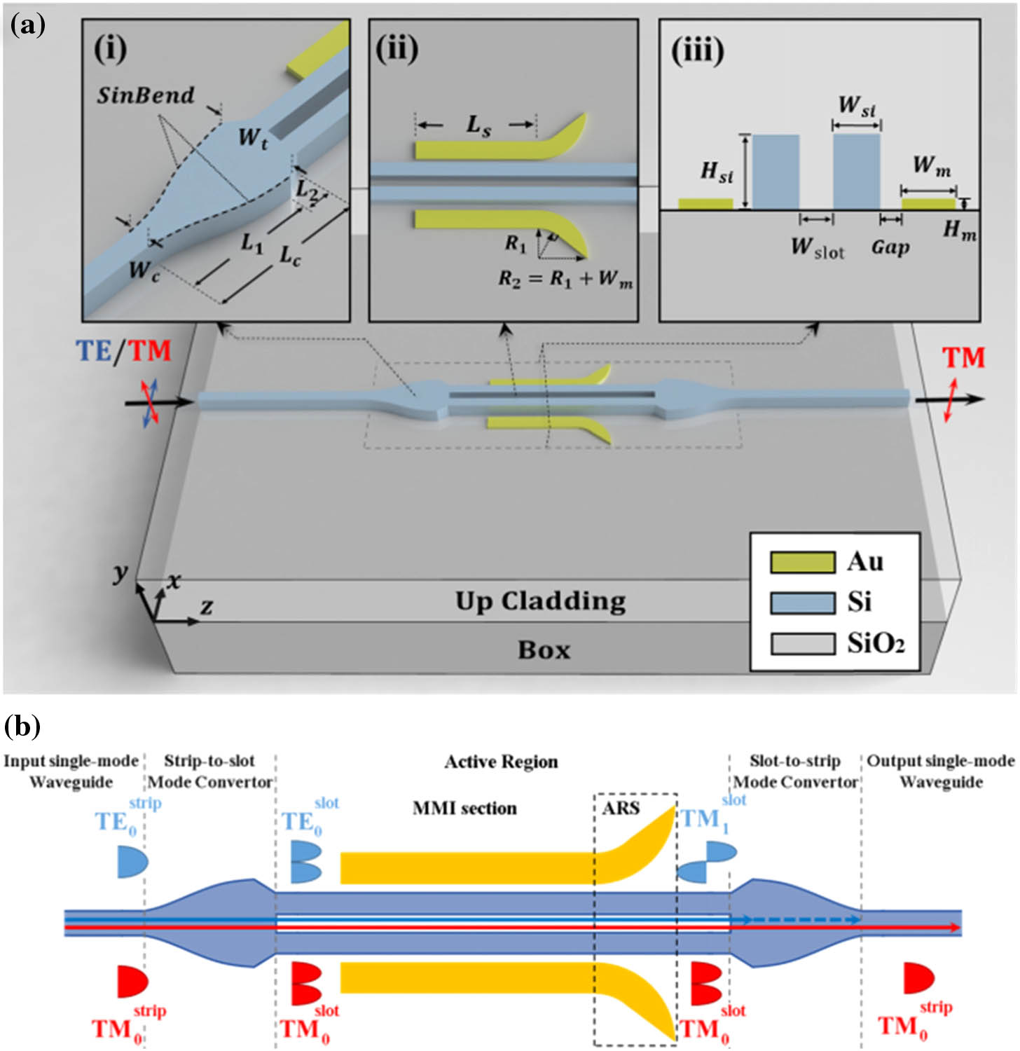
    Fig. 1. (a) Schematic of the proposed TM-pass polarizer. Inset: (i) Compact strip-to-slot mode convertor; (ii) HPSW active region; (iii) cross-section of the HPSW. As an example, the widths of “rails” (Wsi) and slot (Wslot) in the HPSW are chosen as 240 and 180 nm, while the width of metal layer (Wm) is chosen as 300 nm. Besides, the inner radius (R1) and outer radius (R2) of the metal “wing” in ARS are set as 500 and 800 nm in our design, respectively. Under this structural configuration, the dielectric slot waveguide supports four eigenmodes: TE0slot, TE1slot, TM0slot, and TM1slot. (b) The polarization-dependent mode-conversion process in the proposed device.
    Transverse magnetic-field profile of (a) EM2, (b) EM4, and (c) EM5. Black arrows represent the electrical field directions. Corresponding power coupling ratios of (d) EM2, (e) EM4, and (f) EM5 with sweeping Gap and Hm when TE0slot is injected into the HPSW. The mode profiles for TE0slot, EM2, EM4, and EM5 are given under the dimension that Wsi=240 nm, Wslot=180 nm, Wm=300 nm, Gap=45 nm, and hAu=45 nm.
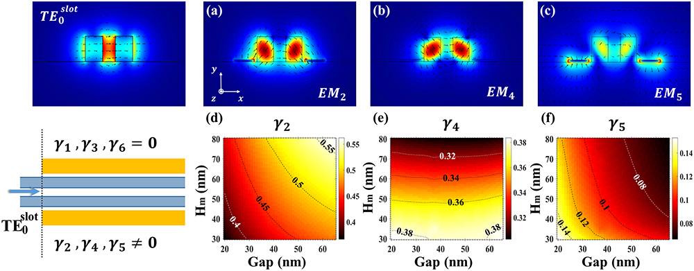
    Fig. 2. Transverse magnetic-field profile of (a) EM2, (b) EM4, and (c) EM5. Black arrows represent the electrical field directions. Corresponding power coupling ratios of (d) EM2, (e) EM4, and (f) EM5 with sweeping Gap and Hm when TE0slot is injected into the HPSW. The mode profiles for TE0slot, EM2, EM4, and EM5 are given under the dimension that Wsi=240  nm, Wslot=180  nm, Wm=300  nm, Gap=45  nm, and hAu=45  nm.
    Transverse magnetic-field profile of (a) EM1, (b) EM3, and (c) EM6. Black arrows represent the electrical field directions. Corresponding power coupling ratios of (d) EM1, (e) EM3, and (f) EM6 with sweeping Gap and Hm when TM0slot is injected into the HPSW. The mode profiles for TM0slot, EM1, EM3, and EM6 are given under the dimension that Wsi=240 nm, Wslot=180 nm, Wm=300 nm, Gap=45 nm, and hAu=45 nm.
    Fig. 3. Transverse magnetic-field profile of (a) EM1, (b) EM3, and (c) EM6. Black arrows represent the electrical field directions. Corresponding power coupling ratios of (d) EM1, (e) EM3, and (f) EM6 with sweeping Gap and Hm when TM0slot is injected into the HPSW. The mode profiles for TM0slot, EM1, EM3, and EM6 are given under the dimension that Wsi=240  nm, Wslot=180  nm, Wm=300  nm, Gap=45  nm, and hAu=45  nm.
    (a) Mode overlap ratio after taking logarithm between the mode field on the termination facet of MMI section and TE0slot in the output dielectric slot waveguide. (b) Corresponding Lm with Gap and Hm varied. (c) Comparison between the mode overlap ratio with and without ARS.
    Fig. 4. (a) Mode overlap ratio after taking logarithm between the mode field on the termination facet of MMI section and TE0slot in the output dielectric slot waveguide. (b) Corresponding Lm with Gap and Hm varied. (c) Comparison between the mode overlap ratio with and without ARS.
    Insertion loss of the strip-to-slot mode convertor (ILc) varied with respect to Wt (for TM0 incidence). Inset: The transverse magnetic field evolution in the proposed strip-to-slot mode convertor and its schematic diagram of structural parameters.
    Fig. 5. Insertion loss of the strip-to-slot mode convertor (ILc) varied with respect to Wt (for TM0 incidence). Inset: The transverse magnetic field evolution in the proposed strip-to-slot mode convertor and its schematic diagram of structural parameters.
    Electric-field evolution with the corresponding (b), (e) Ex and (c), (f) Hx component in the proposed TM-pass polarizer for (a) TE and (d) TM fundamental input. The operation wavelength is 1550 nm, and the refractive indices for gold, SiO2, and Si are 0.238+11.263i [32], 1.444, and 3.478, respectively. Besides, the minimum mesh of 5 nm in x, y, and z directions is set to obtain accurate and stable results.
    Fig. 6. Electric-field evolution with the corresponding (b), (e) Ex and (c), (f) Hx component in the proposed TM-pass polarizer for (a) TE and (d) TM fundamental input. The operation wavelength is 1550 nm, and the refractive indices for gold, SiO2, and Si are 0.238+11.263i [32], 1.444, and 3.478, respectively. Besides, the minimum mesh of 5 nm in x, y, and z directions is set to obtain accurate and stable results.
    Wavelength dependence of (a) transmissivity, (b) ER, (c) reflection, and (d) IL of the proposed device. ER and IL versus (e) ΔWm and (f) ΔWsi.
    Fig. 7. Wavelength dependence of (a) transmissivity, (b) ER, (c) reflection, and (d) IL of the proposed device. ER and IL versus (e) ΔWm and (f) ΔWsi.
    Ruixuan Chen, Bowen Bai, Zhiping Zhou. Low-loss hybrid plasmonic TM-pass polarizer using polarization-dependent mode conversion[J]. Photonics Research, 2020, 8(7): 1197
    Download Citation