
Zhenxing Sun, Yaguang Wang, Rulei Xiao, Leilei Wang, Yangyang Gong, Yi-Jen Chiu, Xiangfei Chen, "Directly modulated 25 Gbaud/s tunable in-series DFB laser array for WDM systems," Chin. Opt. Lett. 21, 011403 (2023)
- Chinese Optics Letters
- Vol. 21, Issue 1, 011403 (2023)
Abstract
1. Introduction
Wavelength-division-multiplexing (WDM) technology has recently shown great potential in the metro and access networks. WDM networks are expected to be applied in next-generation high-capacity front-haul networks and passive optical networks[1,2]. Wavelength tunable semiconductor lasers are very important components in WDM networks. The lasers with fixed wavelengths are desired to be replaced by tunable lasers for enhancing the network flexibility and reducing the system costs[3,4]. Besides, high-speed modulation per wavelength is required for the increasing data traffic[5]. Tunable lasers with different tuning mechanisms have been investigated and reported, including the tunable distributed Bragg reflector (DBR) lasers, the external-cavity tunable lasers (ECTLs), the Vernier-effect-based tunable lasers, and the multi-wavelength distributed feedback (DFB) laser arrays (MLAs)-based tunable lasers[6–10]. The tunable lasers based on the MLAs are superior for the simple wavelength tuning mechanism and the stable single-mode operations. The conventional multi-wavelength laser arrays are placed in parallel, and an extra optical combiner is monolithically integrated for the one-waveguide light output[11]. The optical power loss is introduced by the optical combiner, and the fabrication process becomes complex for the integration of the passive optical combiner. Thus, the lasers in the multi-wavelength laser arrays are expected to be arranged in series to avoid the use of the optical combiner. However, the single-mode stabilities are deteriorated by the grating crosstalk from the lasers placed in series, and the grating crosstalk becomes quite serious when the wavelength spacing is smaller than the width of the grating stopband, which is typically 3.2 nm in the DFB laser[12]. However, a large temperature range is required to tune the wavelength of interest if the wavelength spacing of the laser arrays is too large. The large temperature tuning range may increase the power consumption of the thermoelectric cooler (TEC), cause a large difference in the laser output power, and accelerate the aging of the device.
Here, we demonstrate a high-speed directly modulated tunable in-series laser array (DMTL) with four integrated lasers, and the Bragg wavelengths of the four lasers are separated by 2.4 nm. A three-section design is utilized to reduce the interference from other lasers and obtain good single-mode properties. Based on the three-section structure, the electro-optic (EO) response bandwidth can be enhanced owing to the reduced modulated cavity length. Meanwhile, the photon intensity stays high along the modulated section owing to the
2. Device Design and Fabrication
2.1. Device design
The key to realizing a high-speed DMTL is to increase the modulation bandwidth and reduce the crosstalk among the gratings of the in-series lasers. The relaxation oscillation frequency (
Sign up for Chinese Optics Letters TOC. Get the latest issue of Chinese Optics Letters delivered right to you!Sign up now
![]()
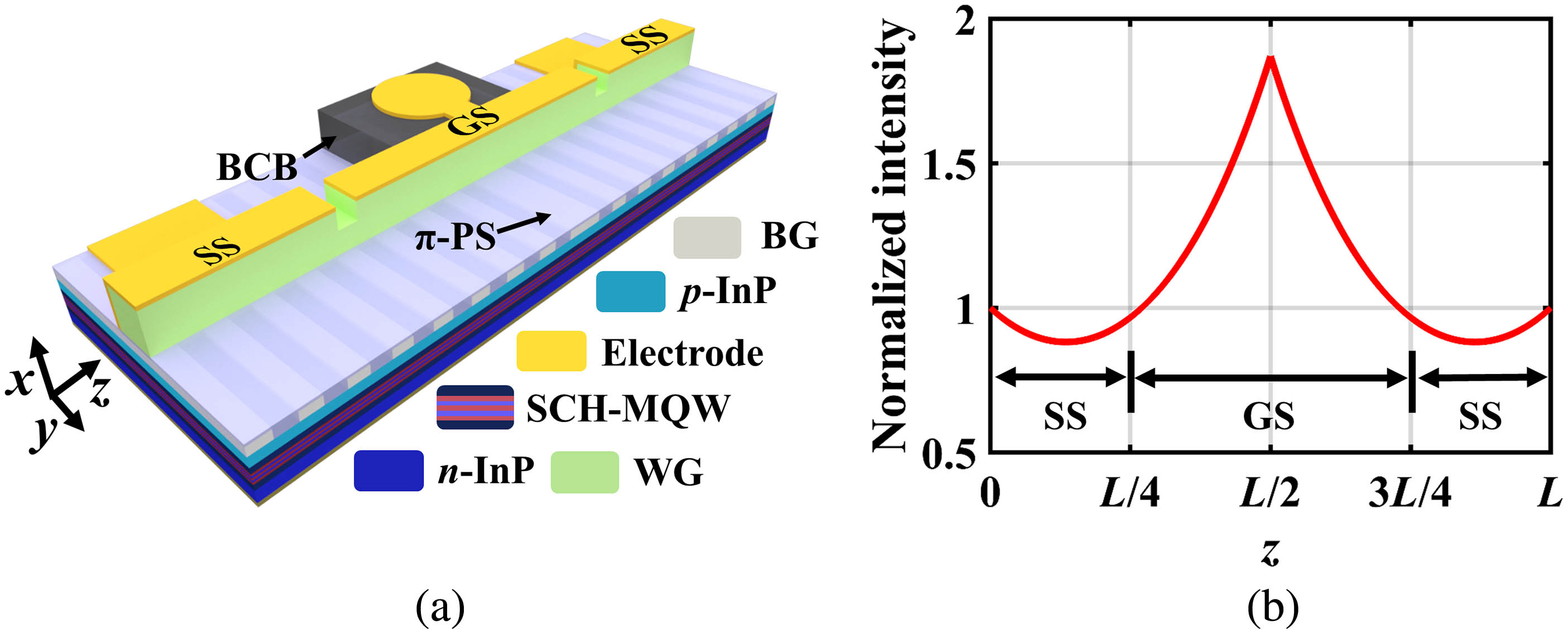
Figure 1.(a) Schematic of the proposed structure of one laser unit and (b) calculated normalized optical intensity of the lasing mode along the cavity of one laser unit. (SS, side section; GS, gain section; SCH-MQW, separate confinement hetero-structure-multi-quantum well; BG, Bragg grating; BCB, benzocyclobutene; WG, waveguide).
In addition, the three-section structure can help suppress the side modes to guarantee the single-mode operations. As shown in Fig. 1(b), the photons of the dominant lasing mode in the cavity are mainly distributed around the center of the cavity, which is different from the side modes. Therefore, the priority of the dominant lasing mode can be increased by the different current injections to the central GS and the SSs. Thus, the single-mode stabilities can be enhanced. Besides, a phase error of the grating in the whole cavity may destroy the single-mode properties, and the grating phase precision can be improved through the REC technique. The REC technique studied in previous work uses a sampled grating to introduce equivalent
![]()
Figure 2.(a) Schematic of the grating designed by the REC technique and (b) sampling periods of the four in-series lasers (π-EPS: equivalent π phase shift).
2.2. Device fabrication
We adopted a standard ridged waveguide structure for the proposed in-series laser array for its simple fabrication process. The compressively-strained InAlGaAs MQW structure is utilized as the active layer for its excellent high-temperature performance. The p-InGaAsP is used as the grating layer. The thickness of the p-InGaAsP grating layer is 50 nm, and the photoluminescence (PL) wavelength of the p-InGaAsP grating layer is 1.36 µm. The coupling coefficient of the uniform grating is approximately
![]()
Figure 3.Picture of the DMTL chip under the microscope (SOA, semiconductor optical amplifier; LD, laser diode).
3. Device Characterization
The proposed DMTL was bonded onto a high-frequency submount to facilitate device characterization. Figure 4(a) shows the fabricated DMTL chip on the submount (COS). AlN is used as the substrate for its high thermal conductivity. The ground coplanar waveguide (GCPW) structure is used to feed the RF signal. The 40 Ω TaN resistor is fabricated for impedance matching. In addition, the RF signals and bias currents are injected separately from two sides. The bias currents are injected into the lasers directly and do not pass the 40-Ω resistors, which effectively decreases the power consumption. The magnetic beads are bonded on the DC line of the substrate to prevent the RF signals.
![]()
Figure 4.(a) Microscopic top view of the DMTL COS and (b) superimposed optical spectra of all four lasers (DMTL, directly-modulated tunable in-series laser array; GCPW, ground coplanar waveguide; COS, chip on submount).
The DMTL COS is placed on a copper carrier, and the temperature of the carrier can be adjusted by the TEC. We analyzed the lasing spectra using the optical spectrum analyzer (Yokogawa, AQ6370). The temperature of the TEC is set at 25°C first. The currents injected to the GS, SS, and SOA (
We studied the impact of
![]()
Figure 5.(a) Optical spectra of LD1 as a function of IGS when ISOA and ISS are both fixed at 30 mA and (b) optical spectra of LD1 as a function of ISS when ISOA and IGS are fixed at 30 and 70 mA, respectively (ISOA, current injected into the semiconductor optical amplifier; IGS, current injected into the gain section; ISS, current injected into the side section).
The typical power-current-voltage (
![]()
Figure 6.(a) Power-current-voltage curve of LD1 with ISOA of 10 mA and (b) laser output power as a function of the ISOA for the four lasers with the IGS and ISS set at 80 and 30 mA (ISOA, current injected into the semiconductor optical amplifier; IGS, current injected into the gain section; ISS, current injected into the side section).
The tunable DFB laser arrays are superior for their simple wavelength tuning mechanism. The wavelength of interest can be obtained by selecting the working laser and adjusting the temperature of the TEC. Here, we tuned 12 channels with 100 GHz spacing for our proposed DMTL.
![]()
Figure 7.(a) Lasing spectra of the tuned 12 channels and (b) tuned temperature of the TEC (left) and SMSRs of all the 12 channels (right) (SMSR, side mode suppression ratio).
The EO response was analyzed using the 70 GHz vector network analyzer (Anritsu MS4647A). The temperature of the TEC is set at 25°C.
![]()
Figure 8.(a) EO response of LD1 when IGS is varied from 40 to 100 mA and (b) EO response of all the four lasers when IGS is 100 mA (GS, gain section; IGS, current injected into the GS).
The 25 Gb/s non-return-to-zero (NRZ) large-signal modulation was performed with a pseudo-random bit sequence (PRBS) of
![]()
Figure 9.Measured back-to-back 25 Gb/s NRZ optical eye diagrams and 25 Gb/s NRZ eye diagrams after 10 km transmission for all 12 channels (Ch., channel; BtB, back-to-back).
![]()
Figure 10.(a) Electrical eye diagram of the 50 Gb/s PAM4 signal after the electrical amplifier and (b) measured 50 Gb/s PAM4 optical eye diagram for channel 10.
4. Conclusion
In this Letter, we demonstrated a 25 Gbaud/s DMTL. High output power (
References
[1] H. Rohde, E. Gottwald, A. Teixeira, J. D. Reis, A. Shahpari, K. Pulverer, J. S. Wey. Coherent ultra dense WDM technology for next generation optical metro and access networks. J. Light. Technol., 32, 2041(2014).
[2] K. Iwatsuki, J. I. Kani, H. Suzuki, M. Fujiwara. Access and metro networks based on WDM technologies. J. Light. Technol., 22, 2623(2004).
[3] J. Buus, E. J. Murphy. Tunable lasers in optical networks. J. Light. Technol., 24, 5(2006).
[4] L. A. Coldren, G. A. Fish, Y. Akulova, J. S. Barton, L. Johansson, C. W. Coldren. Tunable semiconductor lasers: a tutorial. J. Light. Technol., 22, 193(2004).
[5] D. Zhou, D. Lu, S. Liang, L. Zhao, W. Wang. Transmission of 20 Gb/s PAM-4 signal over 20 km optical fiber using a directly modulated tunable DBR laser. Chin. Opt. Lett., 16, 091401(2018).
[6] O. K. Kwon, K. H. Kim, E. D. Sim, H. K. Yun, J. H. Kim, H. S. Kim, K. R. Oh. Proposal of electrically tunable external-cavity laser diode. IEEE Photon. Technol. Lett., 16, 1804(2004).
[7] B. Mason, J. Barton, G. A. Fish, L. A. Coldren, S. P. DenBaars. Design of sampled grating DBR lasers with integrated semiconductor optical amplifiers. IEEE Photon. Technol. Lett., 12, 762(2000).
[8] L. Han, S. Liang, C. Zhang, L. Liqiang Yu, L. Zhao, H. Zhu, B. Wang, C. Ji, W. Wang. Fabrication of widely tunable ridge waveguide DBR lasers for WDM-PON. Chin. Opt. Lett., 12, 091402(2014).
[9] B. Pezeshki, E. Vail, J. Kubicky, G. Yoffe, S. Zou, J. Heanue, P. Epp, S. Rishton, D. Ton, B. Faraji, M. Emanuel, X. Hong, M. Sherback, V. Agrawal, C. Chipman, T. Razazan. 20-mW widely tunable laser module using DFB array and MEMS selection. IEEE Photon. Technol. Lett., 14, 1457(2002).
[10] J. Hong, H. Kim, F. Shepherd, C. Rogers, B. Baulcomb, S. Clements. Matrix-grating strongly gain-coupled (MG-SGC) DFB lasers with 34-nm continuous wavelength tuning range. IEEE Photon. Technol. Lett., 11, 515(1999).
[11] H. Ishii, K. Kasaya, H. Oohashi. Spectral linewidth reduction in widely wavelength tunable DFB laser array. IEEE J. Sel. Top. Quantum Electron., 15, 514(2009).
[12] L. Li, S. Tang, J. Lu, Y. Shi, B. Cao, X. Chen. Study of cascaded tunable DFB semiconductor laser with wide tuning range and high single mode yield based on equivalent phase shift technique. Opt. Commun., 352, 70(2015).
[13] R.-Y. Chen, Y.-J. Chen, C.-L. Chen, C.-C. Wei, W. Lin, Y.-J. Chiu. High-power long-waveguide 1300-nm directly modulated DFB laser for 45-Gb/s NRZ and 50-Gb/s PAM4. IEEE Photon. Technol. Lett., 30, 2091(2018).
[14] G. Liu, G. Zhao, J. Sun, D. Gao, Q. Lu, W. Guo. Experimental demonstration of DFB lasers with active distributed reflector. Opt. Express, 26, 29784(2018).
[15] G. Liu, G. Zhao, G. Zhang, Q. Lu, W. Guo. Directly modulated active distributed reflector distributed feedback lasers over wide temperature range operation. Chin. Opt. Lett., 18, 061401(2020).
[16] R. Nagarajan, M. Ishikawa, T. Fukushima, R. S. Geels, J. E. Bowers. High speed quantum-well lasers and carrier transport effects. IEEE J. Quantum Electron., 28, 1990(1992).
[17] K. Lau, A. Yariv. Ultra-high speed semiconductor lasers. IEEE J. Quantum Electron., 21, 121(1985).
[18] Z. Sun, R. Xiao, Z. Su, K. Liu, G. Lv, K. Xu, T. Fang, Y. Shi, Y. J. Chiu, X. Chen. Experimental demonstration of wavelength-tunable in-series DFB laser array with 100-GHz spacing. IEEE J. Sel. Top. Quantum Electron., 28, 1500308(2022).
[19] Y. Shi, X. Chen, Y. Zhou, S. Li, L. Lu, R. Liu, Y. Feng. Experimental demonstration of eight-wavelength distributed feedback semiconductor laser array using equivalent phase shift. Opt. Lett., 37, 3315(2012).
[20] X. Chen. Precision photonic integration for future large-scale photonic integrated circuits. J. Semicond., 40, 050301(2019).


Set citation alerts for the article
Please enter your email address

© Copyright 2018-2021 | Chinese Laser Press. All Rights Reserved 沪ICP备15018463号-20