R. Dubey1,*, B. Vosoughi Lahijani1, M. H?yrinen2, M. Roussey2..., M. Kuittinen2 and H. P. Herzig1|Show fewer author(s)
Abstract
We experimentally demonstrate the optical properties of gratings engraved in a single-mode waveguide fabricated on top of a dielectric multilayer platform. The structure can be approached as a reflector for Bloch-surface-wave-based two-dimensional optical systems. The gratings have been fabricated on a thin (~λ/25) titanium dioxide layer with a thickness of a few tens of nanometers deposited on the top of a multilayer platform. The optical properties of the gratings have been characterized in the near field with the aid of multi-heterodyne scanning near-field optical microscopy. We investigate the surface wave’s interference pattern, produced by incident and reflected light in front of the gratings. The presented gratings behave as an efficient Bloch-surface–wave-based reflector at telecommunication wavelength.1. INTRODUCTION
For a carefully designed periodic dielectric multilayer, optical surface modes may appear within the photonic bandgap of the periodic multilayer when the periodicity is terminated by a defect layer. These surface electromagnetic modes are called Bloch surface waves (BSWs) [1,2]. The BSWs reveal certain features similar to the well-known surface plasmon polaritons (SPPs). Principally, one of these modes propagates on the multilayer interface to which it is bound while decaying exponentially in the direction perpendicular to this interface, i.e., between the multilayer and the outer medium. Hence, the optical field is confined close to the surface of the multilayer. This vertical confinement makes the BSW a perfect candidate for the design of in-plane/two-dimensional (2D) integrated optics systems and sensors [3–8]. The primary benefit of this in-plane approach is the relaxed fabrication of arbitrary shapes in comparison to standard three-dimensional (3D) integrated photonics structures. 2D optical elements can be produced and used in a few other ways. One of the techniques is addressed by SPPs by structuring a planar metal surface. However, their limited propagation length, due to the strong absorption losses of metal, has hindered the development of SPP-based integrated optics. In the multilayer system presented here, the decay of the amplitude of the surface mode along the propagation direction results from absorption in the material, surface scattering, and leakage into the multilayer because of prism coupling [9,10]. However, due to the low absorption of dielectric materials and the low roughness of the multilayer surface, absorption and scattering do not have a significant contribution to the losses [11,12]. Therefore, the BSW mainly decays due to light leakage into the multilayers in the prism coupling system [13,14]. The decay coefficient of the surface mode due to leakage losses into the multilayer (neglecting the absorption and surface scattering losses) decreases exponentially as the number of periods of the multilayer increases [1]. The propagation length of the BSW has been demonstrated to be in the millimeter range at telecommunication wavelengths [13]. However, this is not the limit; a higher propagation length (several centimeters) might be achieved using grating couplers. Such a long propagation length makes BSWs appealing for miniaturized flat optical components. Moreover, BSW propagation at the surface of the multilayer provides several other advantages. For example, multilayers are wavelength scalable and may be tuned to sustain BSWs over a broad wavelength range from near-UV to IR [6], and there is an ample choice of materials, providing the required transparency and refractive index difference at the desired operating wavelength. In addition, such a platform offers the possibility of tuning the maximum BSW field amplitude at the surface by tailoring the thickness of the topmost layer of the multilayer. The tunability of the field confinement at the surface is attractive for sensing applications, in particular [15]. In addition to all of these advantages, BSWs can sustain electromagnetic modes for both TE and TM polarizations.
With the aim of development of BSW-based optical systems, several 2D optical components used to manipulate BSW propagation have already been studied theoretically and experimentally. They include ridge waveguides, lenses, prisms, diffraction gratings, subwavelength focusers, curved waveguides, disk resonators, and phase-shifted Bragg gratings on top of the multilayer platform [3,14,16–22]. These studies have demonstrated that BSWs can be focused, diffracted, resonated, and totally internally reflected obeying 2D propagation laws. Pioneering research has demonstrated dielectric multilayers sustaining BSWs as a platform for 2D optics. One of the main advantages of the platform concept is the fabrication of thin-film multilayers compatible with a standard wafer-scale production. Further, the topmost layer can be structured to pattern a 2D microsystem using patterning techniques such as e-beam writing and photolithography.
In this work we study the interaction of BSWs propagating through a single-mode 2-μm-wide waveguide along which a grating is patterned. We show that the presented gratings can be used as a BSW reflector at a Bragg wavelength. This work provides an understanding of the fundamental principles of BSW reflection from a dielectric grating and thus represents a step toward the development of BSW-based 2D optical systems. To the best of our knowledge this is the first experimental realization and characterization of a waveguide grating as a BSW reflector at telecommunication wavelength.
Sign up for Photonics Research TOC. Get the latest issue of Photonics Research delivered right to you!Sign up now
2. MULTILAYER PLATFORM AND GRATING DESIGN CONCEPT
The multilayer platform consists of six periods of alternating high- and low-refractive-index materials. The multilayer is designed to support a TE-polarized mode at telecommunication wavelengths around 1553 nm. It consists of layers of silicon dioxide (, ) and silicon nitride (, ). The thicknesses of the layers are 472 and 283 nm for the low- and high-index materials, respectively. A 50-nm-thick layer (defect layer) of has been deposited on the top to terminate the periodicity of multilayer. Henceforth, we address the complete stack (six periods + top layer) as the bare multilayer (BML); see Fig. 1. Further, we deposit an additional layer of 60-nm-thick high-refractive-index material, namely, titanium dioxide (), on top of the BML as a device layer. The refractive index of at a wavelength of 1553 nm is and is transparent in the visible and near-IR regions of the wavelength spectrum. The additional layer of high-index material serves as an efficient device layer that allows the e-beam/lithographical fabrication of 2D photonic devices, for example, the gratings in this study. The BML platform is fabricated by standard plasma-enhanced chemical vapor deposition (PlasmaLab 80+ by Oxford Instruments). Atomic layer deposition (ALD; TFS 200 by Beneq) is used to create the thin film () as a device layer. The accuracy of the thickness and the quality of the material that are possible with the ALD technique are ideal for nanophotonic structures [12]. As was already demonstrated in a previous work, the device layer has a crucial importance in defining the propagation length and the confinement of the surface wave [13], which means that the precision of the deposition of this device layer is a key point of the fabrication process. The fabrication details can be found in Refs. [12,19].
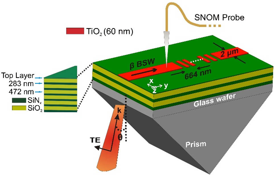
Figure 1.Schematic of the setup of the TIR configuration for BSW coupling with dielectric multilayers deposited on a glass wafer. The 2D grating patterned in the waveguide is fabricated on the top of the multilayers into a 60-nm-thick layer. The SNOM probe, in collection mode, is used to observe the interaction of the BSW with the grating in the near field.
Because of low losses of the constituent dielectric materials, BSW can propagate longer and penetrate deep into the gratings [13]. This provides the advantage of the possibility of improving the reflectivity of the grating by increasing the number of periods of the grating, which is not the case in surface plasmonic gratings. The gratings presented are composed of 80 periods.
3. BSW COUPLING AND CHARACTERIZATION METHODS
To couple BSWs, a total internal reflection (TIR) configuration has been used in order to match the propagation constant of the BSWs. A schematic drawing of the TIR configuration, which is made up of a BK7 glass prism (), is shown in Fig. 1. The laser beam illuminates the sample at an angle with the normal to the platform. This angle is chosen so that the lateral component of the wave vector of incident light matches the following condition: , where is the wave vector of the incident beam, is the wavelength of the incident light in vacuum, and is the propagation constant of the surface mode. A tunable () external cavity diode laser (Agilent, Model 81682A) has been used as the light source in our experiments. We use a focused Gaussian beam to couple light to the BSW, which creates a spot whose projection onto the multilayer surface has a diameter of about 27 μm. According to the schematic presentation of the setup (see Fig. 1), the surface wave propagates in the plane.
As the BSW propagates at the surface of the multilayer, near-field optical microscopy is an optimum method for the characterization of the spatial light distribution of the surface-wave-based optical components. Therefore, to study the interaction of the surface wave with the 2D components, we use a multi-heterodyne scanning near-field optical microscope (MH-SNOM), which collects the evanescent surface waves with a subwavelength aperture probe. The MH-SNOM enables the simultaneous measurement of the amplitude and phase of the near field on the surface of in-plane components. Details about the working principle of the MH-SNOM can be found in Ref. [23].
4. RESULTS AND DISCUSSION
The grating presented in this study has been structured into a 2-μm-wide waveguide, which is patterned in the 60-nm-thick layer of () on top of the multilayer platform. The measured value of the effective refractive indices of the waveguide () and the BML () are approximately 1.20 and 1.14, respectively. According to the Bragg condition , where is the Bragg wavelength, and by choosing a periodicity of with a fill factor of 50% (the slit width and the gap between the slits are set to 332 nm), we obtain a BSW reflector operating at the telecommunication wavelength of 1.553 μm.
In order to investigate the behavior of the waveguide grating at Bragg wavelength, we perform simulations using CST Microwave Studio based on the finite-difference time domain (FDTD) method. Figure 2 demonstrates the simulated field amplitude distribution over the waveguide at another wavelength, , and the Bragg wavelength, .

Figure 2.Simulations using CST Microwave Studio, FDTD method. (a) Field amplitude distribution over the waveguide at a wavelength of , (b) field amplitude distribution over the waveguide at the Bragg wavelength .
In the experiments, at a particular incident angle (larger than the critical angle of 58.26°), the BSW is excited inside the waveguide. We keep the illumination spot approximately 50 μm away from the beginning of the grating. This allows the incident light to well couple to the BSW mode, and therefore to increase the signal-to-noise ratio for measurements along the waveguide. Light propagates in the waveguide and reflects back as it interacts with the gratings. We observe that the field amplitude appears as a standing wave pattern across the waveguide. The standing wave is generated because of the interference of the incident and the backreflected light. The periodicity of the fringes is approximately , with .
We deduce the reflectivity from the contrast of the fringes, which can be defined as [24] where and are the field amplitudes at the point of maximum and consecutive minimum. The reflectivity is linked to the contrast by [25]
Figure 3(a) shows the near-field amplitude distribution along the waveguide at Bragg wavelength . The longitudinal cross section of the surface mode propagating through the waveguide is displayed in Fig. 3(b), where a well-pronounced interference pattern can be seen. We assume the position of the peak amplitude to be the grating input in Figs. 3(a) and 3(b). The peak can be seen as a strong reflection and scattering from the first grating slit. To measure the fringe contrast, a high-resolution scan (20 points/μm in the direction) is performed at around 30 μm before the grating. We normalize the field amplitude to the mean of the fringes at this point, in Fig. 3(b). The high-resolution area is indicated by a black rectangle in Fig. 3(a). Figures 3(c) and 3(d) represent the amplitude distribution of the interference pattern and its corresponding longitudinal cross section plot at . In Fig. 3(d), the fringes are oscillating with a periodicity of 0.63 μm. In theory, the periodicity of the interference fringes produced by a standing wave is defined by . The calculated value of is approximately 0.65 μm. The value of the measured periodicity of the fringes is very close to the theoretical value. The phase of a standing wave with a periodicity of is shown in Fig. 3(e). As expected for a standing wave, one can recognize the classical phase jumps from to and vice versa.
Figure 3.Near-field images acquired by MH-SNOM at the Bragg wavelength . (a) Field amplitude distribution over the waveguide grating; (b) cross section of the field amplitude in the direction, along the waveguide; (c) high-resolution amplitude scan in the area indicated by the black rectangle in (a); (d) cross section of the field amplitude in the direction of (c); (e) measured corresponding phase plot representing a standing wave generated by the interference of the incident and the backreflected BSW mode.
The contrast of high-resolution interference fringes has been calculated using Eq. (1). The average contrast over 13 oscillations is measured to be . It yields a measured reflectivity at . It can be observed in Fig. 3(b) that the field amplitude transmitted through the slits vanishes quickly inside the grating in the Bragg regime. The calculated value of the reflectivity from the contrast, , of the simulated fringes [Fig. 2(b)] is at .
The transmissivity can be deduced from the field amplitude cross section along the waveguide in Fig. 3(a). The estimated transmissivity with respect to the point around 30 μm away from the grating is 0.25%. Considering the law of energy conservation, one can estimate that 28% of the incoming light will be damped. The reason for the damping might be the out-of-plane scattering into the air due to a mismatch between the field profiles of the waveguide grating and the waveguide modes, leakage into the substrate, and scattering due to the roughness of the side walls of the waveguide. However, for the design of the waveguide grating under study, the effective refractive index difference (or the strength of the waveguide grating) is rather small. Therefore, the out-of-plane scattering does not contribute significantly to the losses.
The measured propagation losses inside the nonstructured waveguide are approximately 0.035 dB/μm. The propagation losses in the waveguide are predominantly caused by the roughness of the side walls of the waveguide. In free space, we achieve propagation lengths in the millimeter range, as explained in the introduction section [13]. One can estimate propagation losses of about 26% in the nonstructured waveguide at . However, measured propagation losses inside the structured waveguide are 28%. These calculations indicate that the major contribution to the total propagation losses is because of the surface roughness at the side walls.
We perform a fast Fourier transform (FFT) on the complex field of the high-resolution amplitude scan in Fig. 3(c) at . As expected, the peaks corresponding to two counterpropagating BSWs have been identified; see Fig. 4. The counterpropagating BSWs have the same wavenumber (), with a phase shift of rad. Further, the reflectivity can be deduced from the corresponding amplitude of the counterpropagating BSWs. The estimated reflectivity is 73%, which is very close to what we have calculated from measured contrast of the fringes (72%).
Figure 4.Fourier spectrum computed on the complex field amplitude of the interference fringes [in Fig. 3(c)] at the Bragg wavelength . The peaks corresponds to the wavenumbers () of two counterpropagating BSWs.
Further, we perform the measurements at another wavelength, , following the same procedure as for the Bragg wavelength, . The near-field amplitude distribution along the waveguide is shown in Fig. 5(a) and the corresponding cross section in Fig. 5(b). On the high-resolution scan [see Figs. 5(c) and 5(d)], only very weak interference fringes can be seen. The value of the measured contrast (averaged over 13 oscillations) is . A very-low-contrast fringe pattern can be attributed to a weak backreflection of the incident BSW and hence a low reflectivity, which is evident from the amplitude distribution shown in Fig. 5(a). Light propagates through the waveguide with the least effect (no reflection) of the presence of the grating. The calculated corresponding value of the reflectivity, from the measured contrast, is approximately 1% at . In a similar manner, we find the calculated value of the reflectivity from the contrast, , of the simulated fringes [Fig. 2(a)] to be at . The reason behind the difference between the simulation results and the experimental results is the propagation losses inside the waveguide, which are not considered in the simulations, such as the roughness of the side walls of the waveguide and leakage into the multilayer.
Figure 5.Near-field images acquired by MH-SNOM at a wavelength of . (a) Field amplitude distribution over the waveguide grating; (b) cross section of the field amplitude in the direction along the waveguide; (c) high-resolution amplitude scan in the area indicated by the black rectangle in (a); (d) cross section of the field amplitude in the direction of (c); (e) phase plot showing propagating plane wave behavior that indicates very weak reflection at 1500 nm.
We perform the phase measurement 30 μm before the gratings [see Fig. 5(e)]. We obtain a phase plot signature of a propagating plane wave without the influence of the interference of backreflected light because of a very weak reflection, proving that the measurement is done at a wavelength other than the Bragg wavelength. The estimated transmissivity from the field amplitude plot in Fig. 5(b) is around 52%. As explained above, the estimated total propagation losses are about 47%, with a major contribution from the scattering at the side walls of the waveguide (41% for the nonstructured waveguide). The propagation losses are higher for the wavelength , where light transmits throughout the waveguide grating. This is because the light propagates longer (than in reflection) and passes through the gratings, which results in higher propagation losses, mainly due to the roughness at the side walls of the waveguide, and also because of scattering due to the presence of the gratings.
5. CONCLUSION
In summary, a waveguide grating engraved into a BSW-based waveguide has been realized and experimentally analyzed as a flat reflector at telecommunication wavelength. The grating has been patterned in a 2-μm-wide waveguide by e-beam lithography. An MH-SNOM has been used to map the near-field amplitude distribution of a BSW propagating along the structure. The waveguide grating shows the expected reflector behavior, with a measured reflectivity of 72% at the Bragg wavelength . The near-field images of the grating show high-contrast interference fringes at . This standing wave pattern has been found to arise from the interference of two counterpropagating BSWs. We have also shown that a very low contrast can be attributed to weak backreflection and hence to a low reflectivity at another wavelength, . The FDTD simulations and near-field measurements confirm that the waveguide grating works as a reflector at telecommunication wavelength (). We believe that this study represents a step forward in the development of BSW-based 2D optical systems.
References
[1] P. Yeh, A. Yariv, A. Y. Cho. Optical surface waves in periodic layered media. Appl. Phys. Lett., 32, 104-105(1978).
[2] M. Liscidini, J. E. Sipe. Enhancement of diffraction for biosensing applications via Bloch surface waves. Appl. Phys. Lett., 91, 253125(2007).
[3] T. Sfez, E. Descrovi, L. Yu, M. Quaglio, L. Dominici, W. Nakagawa, F. Michelotti, F. Giorgis, H. P. Herzig. Two-dimensional optics on silicon nitride multilayer: refraction of Bloch surface waves. Appl. Phys. Lett., 96, 151101(2010).
[4] E. Descrovi, T. Sfez, M. Quaglio, D. Brunazzo, L. Dominici, F. Michelotti, H. P. Herzig, O. J. F. Martin, F. Giorgis. Guided Bloch surface waves on ultrathin polymeric ridges. Nano Lett., 10, 2087-2091(2010).
[5] M. Shinn, W. M. Robertson. Surface plasmon-like sensor based on surface electromagnetic waves in a photonic band-gap material. Sens. Actuators B, 105, 360-364(2005).
[6] K. V. Sreekanth, S. Zeng, J. Shang, K.-T. Yong, T. Yu. Excitation of surface electromagnetic waves in a graphene-based Bragg grating. Sci. Rep., 2, 737(2012).
[7] F. Giorgis, E. Descrovi, C. Summonte, L. Dominici, F. Michelotti. Experimental determination of the sensitivity of Bloch surface waves based sensors. Opt. Express, 18, 8087-8093(2010).
[8] A. Sinibaldi, N. Danz, E. Descrovi, P. Munzert, U. Schulz, F. Sonntag, L. Dominici, F. Michelotti. Direct comparison of the performance of Bloch surface wave and surface plasmon polariton sensors. Sens. Actuators B, 174, 292-298(2012).
[9] I. V. Soboleva, E. Descrovi, C. Summonte, A. A. Fedyanin, F. Giorgis. Fluorescence emission enhanced by surface electromagnetic waves on one-dimensional photonic crystals. Appl. Phys. Lett., 94, 231122(2009).
[10] V. V. Moskalenko, I. V. Soboleva, A. A. Fedyanin. Surface wave-induced enhancement of the Goos-Hänchen effect in one-dimensional photonic crystals. J. Exp. Theor. Phys. Lett., 91, 382-386(2010).
[11] E. Bontempi, L. E. Depero, L. Sangaletti, F. Giorgis, C. F. Pirri. Growth process analysis of a-Si1-xNx:H films probed by X-ray reflectivity. Mater. Chem. Phys., 66, 172-176(2000).
[12] M. Hayrinen, M. Roussey, V. Gandhi, P. Stenberg, A. Saynatjoki, L. Karvonen, M. Kuittinen, S. Honkanen. Low-loss titanium dioxide strip waveguides fabricated by atomic layer deposition. J. Lightwave Technol., 32, 208-212(2014).
[13] R. Dubey, E. Barakat, M. Häyrinen, M. Roussey, S. Honkanen, M. Kuittinen, H. P. Herzig. Experimental investigation of the propagation properties of Bloch surface waves on dielectric multilayer platform. J. Eur. Opt. Soc., 13, 1-9(2017).
[14] L. Yu, E. Barakat, T. Sfez, L. Hvozdara, J. Di Francesco, H. P. Herzig. Manipulating Bloch surface waves in 2D: a platform concept-based flat lens. Light Sci. Appl., 3, 1-7(2014).
[15] V. N. Konopsky, E. V. Alieva. Photonic crystal surface waves for optical biosensors. Anal. Chem., 79, 4729-4735(2007).
[16] L. Yu, E. Barakat, J. Di Francesco, H. P. Herzig. Two-dimensional polymer grating and prism on Bloch surface waves platform. Opt. Express, 23, 31640-31647(2015).
[17] M.-S. Kim, B. V. Lahijani, N. Descharmes, J. Straubel, F. Negredo, C. Rockstuhl, M. Häyrinen, M. Kuittinen, M. Roussey, H. P. Herzig. Subwavelength focusing of Bloch surface waves. ACS Photon., 4, 1477-1483(2017).
[18] X. Wu, E. Barakat, L. Yu, L. Sun, J. Wang, Q. Tan, H. P. Herzig. Phase-sensitive near field investigation of Bloch surface wave propagation in curved waveguides. J. Eur. Opt. Soc., 9, 14049(2014).
[19] R. Dubey, B. V. Lahijani, E. Barakat, M. Häyrinen, M. Roussey, M. Kuittinen, H. P. Herzig. Near-field characterization of a Bloch-surface-wave-based 2D disk resonator. Opt. Lett., 41, 4867-4870(2016).
[20] R. Dubey, B. V. Lahijani, M.-S. Kim, E. Barakat, M. Häyrinen, M. Roussey, M. Kuittinen, H. P. Herzig. Near-field investigation of Bloch surface wave based 2D optical components. Proc. SPIE, 10106, 101061G(2017).
[21] L. L. Doskolovich, E. A. Bezus, D. A. Bykov. Phase-shifted Bragg gratings for Bloch surface waves. Opt. Express, 23, 27034-27045(2015).
[22] E. A. Bezus, L. L. Doskolovich, D. A. Bykov, V. A. Soifer. Phase modulation of Bloch surface waves with the use of a diffraction microrelief at the boundary of a one-dimensional photonic crystal. J. Exp. Theor. Phys. Lett., 99, 63-66(2014).
[23] T. Sfez, E. Descrovi, L. Yu, D. Brunazzo, M. Quaglio, L. Dominici, W. Nakagawa, F. Michelotti, F. Giorgis, O. J. Martin. Bloch surface waves in ultrathin waveguides: near-field investigation of mode polarization and propagation. J. Opt. Soc. Am. B, 27, 1617-1625(2010).
[24] J.-C. Weeber, Y. Lacroute, A. Dereux. Near-field characterization of Bragg mirrors engraved in surface plasmon waveguides. Phys. Rev. B, 70, 235406(2004).
[25] A. Drezet, A. L. Stepanov, A. Hohenau, B. Steinberger, N. Galler, H. Ditlbacher, A. Leitner, F. R. Aussenegg, J. R. Krenn, M. U. Gonzalez, J.-C. Weeber. Surface plasmon interference fringes in back-reflection. Europhys. Lett., 74, 693-698(2006).


