We propose a pseudospin-field-dependent waveguide (PFDW) by constructing a sandwiched heterostructure consisting of three magneto-optical photonic crystals (MOPCs) with different geometric parameters. The upper expanded MOPC applied with an external magnetic field has broken time-reversal symmetry (TRS) and an analogous quantum spin Hall (QSH) effect, while the middle standard and the lower compressed ones are not magnetized and trivial. Attributed to the TRS-broken-QSH effect of the upper MOPC, the topological large-area one-way transmission that uniformly distributes over the middle domain is achieved and exhibits the characteristics of a pseudospin-field-momentum-locking; i.e., pseudospin-down (or pseudospin-up) leftward (or rightward) waveguide state when the positive (or negative) magnetic field is applied on the upper MOPC. We further demonstrate the strong robustness of the PFDW against backscattering from various kinds of defects. In addition, a topological beam modulator that can compress or expand the light beam, and a large-area pseudospin beam splitter have been designed. These results have potential in various applications such as sensing, signal processing, and optical communications.
1. INTRODUCTION
In recent decades with the booming development of topological photonics, researchers have studied various topological photonic edge states by analogy to multiple Hall effects in condensed matter physics, such as the quantum Hall (QH) effect, the quantum spin Hall (QSH) effect, and the quantum valley Hall effect [1–8]. The crucial point of 2D one-way transmission in the QH system is the presence of an external magnetic field imposed in magneto-optical photonic crystal (MOPC) and the resulting broken time-reversal symmetry (TRS), exhibiting quantized Hall conductance associated with the topological invariant of the integer Chern number to characterize the topological property of the corresponding photonic bands [9–11]. The prediction of chiral edge states for electromagnetic (EM) waves was theoretically and experimentally accomplished in 2D MOPC systems based on the integer QH effect and extended to the classical wave systems. Extensive studies have revealed that researchers explore considerable functional applications in QH system, including optical add-drop filters, optical switches, slow light, and beam splitters [12–17]. In contrast to the QH effect, the QSH effect based on the Kane–Mele model was proposed using an ordinary PC built with C6v symmetry [18–21], together with Kramers’ degeneracy at the Dirac point to preserve pseudo-TRS. In the QSH system, the pseudospin-dependent helical edge state was achieved by compressing and expanding the honeycomb lattice of PCs, associated with pseudospin-up and pseudospin-down states carrying opposite quantized Hall conductivities. Both the chiral edge state and helical edge state allow for the one-way propagation of EM waves, possessing robustness against defects protected by the bulk topology. Shortly afterward, extensive research theoretically demonstrated the transport behaviors of one-way edge states under the simultaneous interaction of the geometric parameters and external magnetic fields in TRS-broken-QSH systems [22–25], broadening a new realm for topological photonics and electromagnetic devices. Such edge states achieved in the MOPC system facilitate EM waves transporting unidirectionally and are verified to possess strong robustness against obstacles.
To the best of our knowledge, most previous efforts have been devoted to the topological chiral edge state and helical edge state localized at the interference between two wall structures, enabling a platform that the EM wave can transport with high transmittance. Typical well-studied cases include conventional chiral edge states in MOPC systems, classical helical edge states in PC systems, and some novel edge states such as antichiral edge states in a honeycomb lattice [3,15,19,26,27]. However, such waveguides provide a fixed number of channels supporting one-way transmission of EM waves, limiting the modulation of energy channels. Subsequently, recent studies have shown that a topological waveguide with a tunable transmission width can be achieved by introducing a PC heterostructure, which has one domain with the presence of a Dirac cone sandwiched between two domains with different topological invariants [28–31]. Nevertheless, it is desirable to construct heterostructure waveguides inheriting the properties of field-momentum locking in the QH system and pseudospin-momentum locking in the QSH system, providing an efficient scheme to manipulate the transmission behaviors of EM waves.
In this work, we have proposed a 2D pseudospin-field-dependent waveguide (PFDW) heterostructure consisting of three domains; the middle domain features a Dirac cone sandwiched between two MOPCs with different topological invariants in honeycomb lattice. This type of structure supports topological large-area one-way propagation based on the TRS-broken-QSH effect resulting from the broken TRS and the deformation of the upper magnetized MOPC. The momentum of the topological large-area transmission in the PFDW is locked by both pseudospin orientation and the direction of external magnetic field; i.e., pseudospin-down leftward waveguide state under a positive magnetic field and pseudospin-up rightward waveguide state under a negative magnetic field. In addition, the capacity of transmission in a width-tunable PFDW depends on the number of layers in the middle domain with the Dirac cone. Both the pseudospin-down and pseudospin-up states are strongly robust against backscattering from void defects, perfect electric conductor (PEC) defects, and bends. Furthermore, a topological beam modulator and a large-area pseudospin beam splitter have been designed.
Sign up for Photonics Research TOC. Get the latest issue of Photonics Research delivered right to you!Sign up now
2. PFDW MODEL AND BAND STRUCTURE ANALYSIS
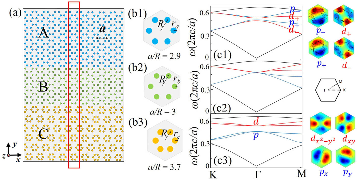
Figure 1(a) shows the PFDW consisting of three domains labeled as , , and colored by three different colors. Each domain consists of a 2D symmetrical MOPC with the same lattice constant; i.e., . The unit cell of each MOPC is composed of six yttrium iron garnet (YIG) rods with a dielectric constant , as shown in Figs. 1(b1)–1(b3). The distance between the center of a rod and the center of its lattice is , which is different for each domain; i.e., in the , , and domains, respectively. It should be pointed that the case of is the standard honeycomb structure, while those cases of or correspond to expansion or compression structures. The number of layers in domains , , and is 6, 4, and 6 in the direction. The YIG rods in domain are magnetized by an external magnetic field of or along the or axis. Therefore, the gyromagnetic anisotropy of YIGs is induced to break time-reversal symmetry and the relative permeability tensor becomes [4,9,32,33] where and . Here, is the resonance frequency, is the gyromagnetic ratio, is the characteristic circular frequency with being the saturation magnetization, and is the damping coefficient. We chose an operation frequency in a low dispersion region that is far away from the resonance frequency, and used and corresponding to the response of YIG at 14 GHz and static magnetic field. The YIG rods in domains and are nonmagnetized. To ensure that the and domains with different topological invariants and configurations can share the common photonic bandgaps, the radius of each of the YIG rods in the , , and domains is set to be , , and , respectively.
Figure 1.Schematic of the PFDW structure and band structure. (a) PFDW structure consisting of domains (blue), (green), and (yellow) with different configurations. The supercell used to calculate the projected band structure is denoted by a red rectangle in (a). (b1)–(b3) Illustration of honeycomb unit cells. (c1)–(c3) Corresponding bulk band structures of domains , , and when domain is biased by . The eigenfields of photonic orbitals at the point hosted by the lattices and are presented on the right.
The band structures of units , , and were calculated using the finite element method (FEM) and are shown in Figs. 1(c1)–1(c3). Only TM polarization with the -field parallel to YIG rods was considered and we adopted normalized frequency throughout this work. Absorbing boundary conditions and periodic boundary conditions were applied to the upper and lower, left and right sides of the supercell, respectively. As shown in Fig. 1(c2), at the point, the fourfold degeneracy of the Dirac cone at exists in unit with no band gap. For domain , the band inversion between the state and state occurs by expanding the honeycomb lattice [Fig. 1(c1)] with the external magnetic field of , which changes the frequency range of this band gap from to . The eigenmode functions at Dirac cone can be classified as , , , and based on spatial parities and pseudospin basis states; therefore, and are formed, and the corresponding Poynting vectors and field patterns are shown on the right of Fig. 1(c1). The clockwise and counterclockwise patterns of the Poynting vector in a unit cell correspond to the pseudospin-down and pseudospin-up states [22,34,35]. Since the YIG lattices in domain are geometrically expanded and immersed in the external magnetic field, domain shows the property of TRS-broken-QSH insulator. Alternatively, for domain shown in Fig. 1(c3), the Dirac cone splits into two pairs of two-fold degenerate (blue) and (red) states by compressing the honeycomb lattice to create a band gap of [the bandgap width between states and states is ], the field patterns of degenerate and states are shown on the right side of Fig. 1(c3) and no band inversion appears. To characterize the topology property of the band, we introduced the spin Chern number, which was first proposed by Sheng et al. and has been proven to be valid when the time reversal invariance is broken [36–38]. A perturbation Hamiltonian is introduced because of the presence of the external magnetic field
The spin Chern number can be evaluated by
and are model parameters defined by the coupling coefficients [23,39]. In domain , , and . The spin Chern number of unit becomes and , where the signs of and in correspond to pseudospin-up and pseudospin-down components with external magnetic fields of and , respectively, indicating that the corresponding band gap is topologically nontrivial and the PDFW supports spin-momentum locking propagation with topological protection. Differently, for domain () with no external magnetic field, and the corresponding spin Chern number is , which is topologically trivial. Besides, the presence of the Dirac cone of domain is not broken.
To explore the properties of waveguide states in a PFDW structure, we further calculated the projected band structure and eigenmodal field. Here, we considered two cases of Fig. 1(a), where the YIG rods in domain were immersed in a magnetic field of 2900 G with opposite directions, respectively. Figure 2(a) shows the projected band gap from to for the PFDW applied by (red) and (blue). We first discuss the case of Fig. 1(a), where domain is immersed in . For this case, domains and carry spin Chern number of and , respectively. As analyzed above, for pseudospin-up component, domains and have the same topological invariants of zero; i.e., . The system is trivial so that no one-way state associated with pseudospin-up polarization is supported. While for the pseudospin-down component, the spin Chern numbers for domains and are and 0 (i.e., , indicating that the topological properties on both sides of domain have discontinuous changes to support one-way transmission of the pseudospin-down component. Likewise, when domain is immersed by , only for pseudospin-up polarization, the difference of spin Chern numbers between domains and is nonzero (i.e., ), which supports the existence of a topological one-way mode in domain .
Figure 2.Projected band gap and the eigenmodal field distributions () of the PFDW. (a) Projected band structures of the PFDW in the cases of (red) and (blue). The black dashed line denotes the typical frequency () that intersects with the red and blue dispersion curves at points 1 () and 2 (), respectively. The red and blue triangles represent pseudospin-down and pseudospin-up states. (b) and (c) Eigenfield distributions and the time-averaged Poynting vector of the supercell corresponding to points 1 and 2. The red and blue arrows indicate waveguide states propagating in negative and positive directions, respectively.
As illustrated in Fig. 2(a), the corresponding dispersion curve represents the one-way waveguide state located in photonic band gap when domain is applied with an external magnetic field. The slopes of the blue and red dispersion curves mean that the group velocities for the cases of domain applied with and are always positive and negative, respectively. As a result, the EM waves excited at the modes of the red () and blue () curves will propagate leftward and rightward with opposite group velocity, respectively. The eigenfields at points 1 and 2 at () are depicted in Figs. 2(b) and 2(c); the time-averaged Poynting vectors for unit marked by the red rectangles are also shown in these figures. The clockwise and counterclockwise patterns of the Poynting vectors for points 1 and 2 correspond to the characteristic of pseudospin-down and pseudospin-up states, indicating that the PFDW with supports pseudospin-down leftward/pseudospin-up rightward one-way states, respectively, which verifies our analyses above.
Therefore, the physical mechanism of the topological waveguide state is attributed to the TRS-broken-QSH effect because of the external magnetic field and geometric deformation of lattice. It should be emphasized that the geometric deformation of lattice cannot be ignored because it provides the competition between the broken TRS and broken spatial inversion symmetry. Obviously, the PFDW exhibited the properties of both pseudospin-momentum locking in a conventional helical edge state and magnetic field-momentum locking in conventional chiral edge state. In particular, different from the edge state existing at the interface between two topological inequivalent materials, the eigenfields at points 1 and 2 were topological large-area waveguide states, which means that the PFDW supported EM waves to pass through the entire bulky domain and carry more energy and information compared to classical edge states [3,19,26,27].
We additionally calculated the relation between the topological frequency window and the layer amount of domain (). The corresponding eigenfield distributions with the specific number of layers in domain are also demonstrated in Fig. 3. As shown in Fig. 3(a), the layer amount in domain is increased, and the width of the band gap decreases. Even though the width of the topological frequency window tends to narrow, it remains wide enough for the operation frequency (), even for . In addition, the PFDW still supports the existence of a topological large-area, one-way mode in bulky domain , as seen in Fig. 3(b).
Figure 3.(a) Width of the topological frequency window as a function of the number of layers in domain (). (b) Eigenfield distributions when , 10, 20.
Based on the discussions above, we know that the designed PFDW supports large-area pseudospin-field-dependent transmission; i.e., pseudospin-up state transporting rightward under (domain ) and pseudospin-down state transporting leftward under (domain ). Next, we studied the EM wave transmission behaviors in the PFDW.
As shown in Fig. 4, we set two kinds of sources carrying positive or negative orbital angular momentum (i.e., pseudospin-down or pseudospin-up source) to excite waveguide states in the topological PFDW. For the case of domain applied with , when the pseudospin-down source () is excited [Fig. 4(a)], there is almost no field propagating to the right side because no edge state associated with the pseudospin-down component is allowed. However, when the pseudospin-up source () is excited [Fig. 4(b1)], the field mainly concentrates in the whole domain and propagates one-way rightward, supporting large-area transmission of an EM wave unidirectionally. On the contrary, for the case of domain immersed in , when the pseudospin-up source () is excited [Fig. 4(c)], the field distribution is very weak and almost no EM wave transports in the PFDW; however, the EM wave propagates unidirectionally along the left direction in a helical state when the pseudospin-down source () is excited [Fig. 4(d1)]. Therefore, it is clear that when a magnetic field is applied, the transmission of an EM wave in the PFDW is dependent on the pseudospin orientation of the source. When the identical pseudospin source is used as excitation, the transmission of the PFDW is dependent on the magnetic field. These results agree well with the predictions from Fig. 2.
Figure 4.Transport phenomena of the PFDW. Simulated field distributions for cases of domain immersed in excited by (a) pseudospin-down source and (b1) pseudospin-up source; and in excited by (c) pseudospin-up source and (d1) pseudospin-down source. (b2) and (d2) are Poynting vector distributions of (b1) and (d1) denoted by the red frames. () represents the pseudospin-up (pseudospin-down) source oscillating at .
We then calculated the distribution of the Poynting vectors in Figs. 4(b1) and 4(d1) to study the energy flow of EM waves in domain . As shown in Figs. 4(b2) and 4(d2), counterclockwise and clockwise energy flux vortexes seem to be self-trapped in each unit of six YIG rods and finally exhibited the macroscopic energy flux propagating unidirectionally rightward and leftward, respectively, corresponding to the pseudospin-up and pseudospin-down states in Figs. 4(b1) and 4(d1). Despite very little energy flowing into domain , the vast majority of energy fluxes propagate unidirectionally along four horizontal channels, which is equal to the layer amount of YIG lattices in domain . Obviously, the larger layer amount of YIG lattices in domain , the more channels will be available to decrease the energy density in each layer during the one-way transmission in the PFDW, which can carry more information without damaging the device. These simulation results are consistent with the predictions from the analyses of the projected band structure and eigenfield above.
Notably, if domain is applied with a negative (or positive) magnetic field and the EM wave is radiated from a trivial point source, it will propagate rightward (or leftward) with only pseudospin-up (or pseudospin-down) orientation, as shown in Fig. 5. It can be explained that the other component is suppressed as in Figs. 4(a) and 4(c) because of the broken TRS’s victory over the broken spatial inversion symmetry. Therefore, the waveguide we construct automatically locks with the pseudospin component, providing an additional degree of freedom; i.e., a pseudospin (orbital angular momentum) that can be manipulated in a practical application.
Figure 5.Transport phenomena of the PFDW. Simulated field distributions excited by a trivial point source for cases of domain immersed in (a1) and (b1) . (a2) and (b2) Poynting vector distributions corresponding to (a1) and (b1). (a3) and (b3) are an enlargement of (a2) and (b2) denoted by the black frames. Red star represents the trivial point source oscillating at .
Furthermore, we constructed an intersection channel consisting of domains , , and to verify the one-way transmission. Its upper (or lower) left and right parts are domain (or ), while the crossing part is domain . As shown in Figs. 6(a1) and 6(b1), the boundaries between adjacent domains are marked with black dashed lines. The left sides of domain are immersed in in both configurations, while the applied magnetic fields on the right sides of domain in both configurations are in opposite directions; i.e., in Fig. 6(a1) and in Fig. 6(b1), respectively. Here, we set a pseudospin-up source at the middle of the left boundary of domain (denoted by the red star). When the magnetic fields applied to the left and right domains were in different directions [Figs. 6(a1) and 6(a2)], the EM wave propagated rightward before meeting the intersection point and then turned to propagate unidirectionally along the upper channel [i.e., the waveguide consisting of ] with broken TRS [29]. Note that the right part of domain did not support one-way mode propagating rightward, so the distribution of field on the right side of domain rapidly decreased.
Figure 6.Transport phenomena of EM transmission in PFDW-based topological intersection channel. (a1) and (b1) field distributions of the intersection channel with different distributions of external magnetic fields. (a2) and (b2) Time-average Poynting vector distributions corresponding to (a1) and (b1). Domain applied with and is depicted as blue and red, respectively. Domains and are depicted as green and yellow. (c) Normalized energy intensity distributions measured along the blue and red lines in (a1) and (b1), respectively. The red star on left side represents pseudospin-up source oscillating at .
In the other case shown in Fig. 6(b), where both domains were applied with the same magnetic field of , the EM wave propagated rightward unidirectionally with minimal energy spreading into the neighboring channels. Note that the distribution of field in domain at the right boundary resulted from the imperfect absorption of the scattering boundary. Additionally, we calculated the normalized energy flow density distribution along the blue and red lines in Figs. 6(a1) and 6(b1), respectively. As depicted in Fig. 6(c), the energy intensity of EM wave calculated along the blue line was extraordinarily weak compared to that along the red line, which meant that there was almost no light propagating toward the right side in the case shown in Fig. 6(a1). These results provide powerful evidence that an artificially constructed PFDW structure has potential for large-area one-way propagation and tunable large-area light confinement. PFDW-based channel intersection holds promise for an optical switch by adjusting the magnetic field applied on the upper right domain .
4. ROBUSTNESS ANALYSIS OF PFDW
It is remarkable that domain has the characteristic of unidirectional transmission in certain frequency range, when it is sandwiched between topologically nontrivial domain and topologically trivial domain . We further demonstrated the robustness of the PFDW against various kinds of defects. Three kinds of defects [i.e., void defect, perfect electric conductor (PEC) defect, and bend], were studied. The YIG rods in domain were biased by and a pseudospin-up source was adopted here.
The three kinds of defects were created. The void defect in domain was constructed by removing 4 YIG rods in domain [Fig. 7(a)]. A PEC defect with a length of and thickness of was inserted vertically into domain to block the transmission channel [Fig. 7(b)]. Four sharp bends with large change angles of 120° were created, as shown in Fig. 7(c). The simulation results of field distributions at 0.528() for the three cases are shown in Figs. 7(a)–7(c). They clearly present the smooth one-way propagation of an EM wave in the PFDW after passing through the channel with void defects, a PEC obstacle, and sharp corners, indicating that the backscattering of the one-way waveguide state was nearly suppressed in the PFDW structure. The transmission spectra of EM waves in Fig. 7(d) show that most of the energy goes through the channel with various defects and propagates one-way rightward within the topological frequency range depicted by the shaded area.
Figure 7.Simulated field distributions at in PFDW with (a) void defects, (b) PEC obstacle, and (c) bends. The white block inset in (b) is the corresponding Poynting vector distributions. (d) Simulated transmission spectra in PFDW for three kinds of defects, respectively. Shaded area represents the photonic band gap.
Notably, the large-area PFDW state originated from the TRS-broken-QSH effect here simultaneously exhibits strong robustness against void defects and bends, as well as PEC defects. It is known that in a PC waveguide consisting of pure dielectric materials, the conventional helical edge state protected by TRS is robust against void defects and bends, but not against PEC defects. For the considered structure here, due to the broken TRS of domain resulting from the external magnetic field, an equivalent one-way transport channel between the upper part of the PEC and the neighboring YIG rods is created, as shown by the enlargement inset in Fig. 7(b). Most of the energy flux goes around the upper end of the PEC, and then recovers to strongly concentrate in domain . Finally, it propagates rightward with almost no backscattering, showing strong robustness that distinguishes it from that of a conventional helical edge state. Such strong robustness of the PFDW against various defects provides good tolerance for one-way large-area waveguide fabrication in practice and has potential in versatile applications.
5. DESIGNS OF TOPOLOGICAL BEAM MODULATOR AND PSEUDOSPIN BEAM SPLITTER
The unique transmission behaviors of EM waves in a PFDW provide an excellent platform for the design of various topological devices such as the topological beam modulator and the large-area pseudospin beam splitter we have designed.
First, we designed a topological beam modulator that can compress or expand the light beam width. Compared to conventional helical edge states propagating along the interface, the PFDW supports large-area one-way transmission of an EM wave in domain , which provides more tunable degrees of freedom. The beam modulator consists of two PFDWs with different transmission widths (i.e., the number of YIG layers in domain ). The number of layers in domain is changed from 10 to 1 from the left to right side abruptly [Figs. 8(a1) and 8(b1)].
Figure 8.(a1) and (b1) distributions using a point source excitation at on the left and right boundaries of domain in the PFDW structure, respectively. The number of layers in domain drops from 10 to 1 (from the left to right sides). (a2) and (b2) Normalized intensity distribution measured along the red and blue lines in (a1) and (b1). (c) S21 and S12 are the simulated transmission spectra when the point source is excited from the left and right boundaries of domain , respectively. The red star indicates the point source radiating at .
We used a point source with pseudospin-up (or pseudospin-down) orientation to excite rightward (or leftward) one-way propagation of an EM wave when domain is applied with (or ). The simulated field distributions are shown in Figs. 8(a1) and 8(b1). In Fig. 8(a1), the EM wave excited from the left pseudospin-up source propagates rightward with a beam of 10 layers in the left part, and then is compressed into a narrow beam with one layer in the right part, working as a beam compressor. On the other hand, in Fig. 8(b1), the EM wave excited from the right pseudospin-down source propagates leftward with a beam width of one layer in the right part, and then is expanded into a wide beam with a width about 10 layers in the left part, functioning as a beam expander. The corresponding energy intensities along the red and blue lines are shown in Figs. 8(a2) and 8(b2). They clearly show that the energy density is significantly increased (or decreased) when the EM wave propagates rightward (or leftward) in Fig. 8(a1) [or Fig. 8(b1)]. In addition, the transmission spectra for the beam modulator in both cases are depicted in Fig. 8(c). It shows that the PFDW structure still supports topological one-way propagation of an EM wave even for beam compression and expansion. The tunable configuration and convenient magnetic field bias hold promise for energy transmission modulation for photonic integrated devices.
Next, we propose another potential application of the large-area helical waveguide state based on the unique advantages of PFDW. Here, a pseudospin beam splitter is constructed by two PFDWs combined along the armchair edge, as shown in Fig. 9(a). To separate different pseudospin components, the left and right parts of domain are immersed in and , respectively. Because of the chirality caused by the opposite external magnetic fields, the edge state was only allowed to propagate downward at the interface between the left and right domains ; thus, the energy of the EM wave will be well confined in domain . Therefore, when a point source radiating at was placed at the center of the designed structure, it was expected that the leftward and rightward one-way large-area helical waveguide states with opposite pseudospin orientations would dominate the left and right sides of domain , respectively.
Figure 9.Topological large-area pseudospin splitter. Simulated distributions of (a) field and (b1) and (b2) energy fluxes (time-averaged Poynting vector marked as the red arrows) in PFDW circled by red frames, with metallic obstacles inserted in the left and right sides of (a). (c) Simulated transmission spectra along left boundary and right boundary of the structure. White rectangle and red star denote the PEC obstacle of and the out-of-plane point source, respectively. Shaded area indicates the photonic band gap.
Figure 9(a) shows the simulated transport phenomenon of the topological large-area pseudospin beam splitter. The EM wave radiated from the trivial point source was divided into isolated pseudospin-down and pseudospin-up components to propagate leftward and rightward unidirectionally at both sides of the PFDW, respectively. The energy flux vortexes of the pseudospin-down (leftward) and pseudospin-up (rightward) components were clockwise (green circular arrows) and counterclockwise (blue circular arrows) cycling around YIG clusters. Furthermore, we symmetrically inserted two identical PEC obstacles into domain of the pseudospin beam splitter to demonstrate the robust one-way transport behaviors, as shown in Figs. 9(b1) and 9(b2). It clearly shows that one-way transmissions of EM waves are resumed after passing through the PEC obstacles, and the energy flux vortexes are the same as those before coming across the PEC obstacles. Notably, the energy flux circulations surrounding the PEC obstacles for the left and right parts of domain were counterclockwise and clockwise, maintaining the unidirectional transmission after bypassing the PEC defect under topological protection due to the broken TRS. Figure 9(c) illustrates the transmittance ratio defined as with and the energy fluxes propagating in the left and right directions. It shows that the transmittance ratio is almost zero with little fluctuation in the topological frequency range, indicating that a trivial point source is nearly equally divided into a rightward pseudospin-up component and a leftward pseudospin-down component. Obviously, these simulation results demonstrate the robust one-way transport behaviors and the characteristics of pseudospin-field-momentum locking of the PFDW. The pseudospin beam splitter can work as a power splitter to separate two different pseudospin components to propagate in opposite directions. In addition, if the pseudospin components carry different data information, it also can separate and filter the message, which has potential for sensing and signal processing. It is also expected that the pseudospin splitter and beam modulator can be combined to simultaneously regulate the energy transmission of different pseudospin components.
6. CONCLUSION
In conclusion, we have proposed a PFDW by constructing a sandwiched structure composed of three MOPCs with different magnetization configurations. Based on the TRS-broken-QSH effect from the external magnetic field and geometric deformation from the upper MOPC, the topological large-area helical waveguide state in the PFDW exhibited the property of pseudospin-field-momentum-locking; i.e., pseudospin-down leftward waveguide state under the positive magnetic field and pseudospin-up rightward waveguide state under the negative magnetic field. The freedoms of pseudospin and magnetic field were introduced in the PFDW, among which the former one was intrinsic, while the latter one was external. It is possible to excite and receive the specific internal information (i.e., pseudospin orientation) of large-area transmission by adjusting the external field, which provides what we believe, to the best of our knowledge, is a new way to manipulate information. It was shown that the capacity of transmission in a width-tunable PFDW depends on the number of layers in domain featuring a Dirac cone, enhancing the degrees of freedom available to manipulate energy and information in MOPC systems. The strong robustness of the large-area transmission in PFDW against various kinds of obstacles including void, PEC, and bend, was also analyzed. Additionally, by taking advantage of the excellent properties of the PFDW, a topological beam modulator and a large-area pseudospin beam splitter with high performances were designed. These results offer an efficient scheme to manipulate light beams and energy in potential applications such as sensing, signal processing, and optical communications.