In this paper, we theoretically propose and experimentally demonstrate the manipulation of a novel degree of freedom in ring resonators, which is the coupling from the clockwise input to the counterclockwise propagating mode (and vice versa). We name this mechanism backcoupling, in contrast with the normal forward-coupling of a directional coupler. It is well known that internal reflections will cause peak splitting in a ring resonator. Our previous research demonstrated that the peak asymmetry will be strongly influenced by the backcoupling. Thus, it is worth manipulating the backcoupling in order to gain full control of a split resonance for the benefit of various resonance-splitting-based applications. While it is difficult to directly manipulate the backcoupling of a conventional directional coupler, here we design a circuit explicitly for manipulating the backcoupling. It can be potentially developed for applications such as single sideband filter, resonance splitting elimination, Fano resonance, and ultrahigh- and finesse.
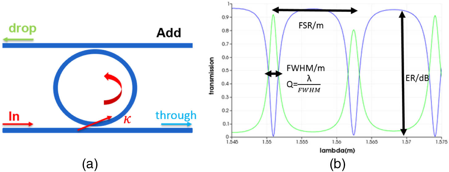
Silicon photonics has grown to be a leading platform for photonic integrated circuits (PICs) thanks to their compatibility with CMOS manufacturing and high index contrast. There are already rich libraries of functional components, and the silicon ring resonator has proven itself as one of the most important and widely used building blocks. Its ultracompact footprint, high -factor, large free spectral range (FSR), and finesse make it a great component for diverse functions such as filters, (de-)multiplexers, laser cavities, optical sensors, and nonlinear optics. The schematic and outputs of an ideal add–drop ring resonator is given in Fig. 1. For a given propagation loss of the waveguide, only three parameters can be manipulated at the design stage of a silicon ring resonator, namely, the total roundtrip length and the two power coupling coefficients at the directional couplers (DCs) . For an add–drop ring resonator, the two DCs are usually designed to be identical (same ) to ensure good working condition [1]. These two parameters, and , determine the performance indicators of such a ring resonator. is responsible for the FSR, while the extinction ratio, the full width at half-maximum (FWHM), and the -factor of the resonance are dependent on both.
Figure 1.(a) Schematic and (b) outputs of an ideal ring resonator.
Previous research has shown that the performance of real silicon ring resonators is dramatically impacted by parasitic effects, most importantly by internal backreflections, no matter what their origin is. One example is the stochastic backscattering induced by the sidewall roughness, which is inevitable for silicon ring resonators fabricated with most current fabrication technologies. For a simple strip waveguide, this backscattering induces stochastic reflections and fluctuations in the transmission spectrum [2,3]. When such a waveguide is used in a ring resonator, the effects become more complicated and pronounced. This backscattering will couple the two circulating modes in a ring resonator, namely, clockwise (CW) and counterclockwise (CCW) propagating modes. In an ideal ring, these are uncoupled and therefore degenerate, so they resonate at the same frequency (wavelength). The degeneracy will be broken when they are coupled; as a consequence, resonance splitting will emerge, with the splitting distance depending on the coupling strength [4,5]. Besides the stochastic backscattering in the waveguides, discontinuities between straight and bend sections, or at the edges of the directional couplers, will also induce backscattering if they are not properly engineered.
Even when backreflections are usually considered to be an inconvenience, there have been efforts to intentionally induce resonance splitting in order to enable novel functionalities. This can be achieved by either putting reflective elements into a ring resonator or using coupled resonators. For instance, placing a reflective element in the ring waveguide to induce resonance splitting can lead to applications like tunable fast and slow light [6,7], novel modulation schemes [8], single sideband generation [9], tunable Fano resonances [10], spectral tuning [11], chirality and exceptional point [12,13], and an optical analogue to electromagnetically induced transparency (EIT) [14]. The use of coupled resonators to induce resonance splitting also shows many applications, including signal processing [15], coupled-resonator-induced transparency [16], differential equation solvers [17], photonic molecules [18,19], optical signal processing [20], etc.
Sign up for Photonics Research TOC. Get the latest issue of Photonics Research delivered right to you!Sign up now
While backreflections cause resonance splitting, and we have demonstrated that this can be actively manipulated [21], it is not the only parasitic effect in a silicon ring resonator. For instance, backreflections alone cannot induce asymmetries in the resonance peaks, which are observed in many real-life ring resonators [5]. In our previous work on silicon ring resonators with backreflections, we concluded that the origin for asymmetric resonance splitting can be found in backcoupling in the directional couplers [5]. The concept of the backcoupling is illustrated in Fig. 2, and the impacts of the backcoupling manipulation can also be mathematically proven, as evident in Eqs. (1)–(6), which are the equations derived from temporal coupled mode theory for the field amplitude at the through-port of an add–drop ring resonator with both backscattering and backcoupling:
Figure 2.(a) Illustration of the backcoupling in a directional coupler. (b) Ring resonator with this backcoupling.
In these, is the resonant frequency of this resonator, and refers to the field reflectivity of the internal reflection that couples CW and CCW modes. and represent the forward-coupling and the backcoupling coefficients in a field, respectively. means the total decay rate of the resonator, including the coupling rates at the directional couplers and the loss rate due to the propagation loss around the ring resonator. Clearly, two resonances and with their own central frequencies and are induced due to the internal reflections. Moreover, the forward-coupling and the backcoupling terms appear in the numerator for the transmission at the through port, and thus they influence the relative height of and .
Just as with backreflections, it can be interesting to manipulate the backcoupling in a ring resonator. To study its influence, we built an optical circuit model in the Caphe circuit simulator provided by Luceda [22,23]. We define an all-pass ring resonator that contains a dimensionless, lumped reflector inside to induce the resonance splitting. The scatter matrix of the directional coupler is manually modified to adjust the backcoupling strength and phase. During this operation, we ensure that the scatter matrix is always unitary and reciprocal. The simulated spectra are given in Fig. 3. For simplicity, we use a term to indicate the ratio between the backcoupling and forward-coupling. Clearly shown in Fig. 3(a), varying the backcoupling strength can significantly alter the peak asymmetry; Fig. 3(b) shows that adding a minus sign to , which means phase difference between and , can determine which peak is manipulated. While when , namely , the resonance splitting disappears, as shown in Fig. 3(c). In summary, manipulating the resonance splitting by tuning the backcoupling can provide a further degree of freedom for those applications taking advantage of the resonance splitting. Moreover, backcoupling manipulation could be developed into applications such as sideband filters and elimination of backscattering-induced resonance splitting. We will also show that it can generate a Fano resonance as well as resonances with ultrahigh- and large finesse.
Figure 3.(a)–(c) Simulations of an all-pass ring resonator with a lumped reflector inside and the backcoupling at the directional coupler. (d) Schematic. is the ratio of backcoupling over forward-coupling, .
In the introduction, we provided an explanation for what the backcoupling is and how it will influence the resonance with visible splitting. In previous simulations, we managed the backcoupling by means of manually modifying the scatter matrix of a directional coupler. However, it is impractical to directly introduce a controllable backcoupling to a conventional directional coupler. In order to make the manipulation of the backcoupling realistic, we designed the circuit shown in Fig. 4. It consists of two parts: a tunable Mach–Zehnder interferometer (MZI) that splits incoming light into two paths (in1 and in2) and a ring resonator that accepts both of these two paths as inputs for the CCW and CW modes. Therefore, in the absence of any other source of backscattering and backcoupling, each of these two inputs will contribute to one circulating mode of the ring resonator. Thus, the split ratio of the MZI determines how much incoming light will be coupled to each circulating mode. Two phase shifters (PSs) are placed in the circuit. One of them (PS1) is on the arm of the MZI, and the other one (PS2) is on one access waveguide of the ring resonator. PS1 is responsible for tuning the split ratio of the MZI; alternatively speaking, it controls the magnitude of the backcoupling. PS2 changes the relative phase difference between two inputs of the ring resonator; in other words, it takes control of the phase difference between and .
Figure 4.Designed circuit in order to introduce manipulation backcoupling in a realistic way. An MZI is placed in front of a ring resonator to dynamically control the intensity of light in two inputs of a ring resonator. Each of the inputs will couple to one circulating mode in the ring.
As previously mentioned, the manipulation of backcoupling only affects the output resonance when it shows splitting, which is induced by internal reflections—and the source for the internal reflections can be either the stochastic backscattering or an intentional reflective element. Thus, we design two varieties of this circuit. One has a circular ring resonator, whose internal reflection purely comes from the stochastic backscattering of the ring waveguide, while the other circuit has a tunable reflector inside the ring resonator. Schematics of the ring with such a reflector and this reflector itself are provided in Fig. 5. Details about such a reflector can be found in Ref. [24]. In short, the reflector consists of a tunable MZI loop mirror, where a phase change can manipulate the reflectivity from 0 to 100%.
Figure 5.Schematics of the ring resonator with (a) a reflector inside and (b) the tunable reflector.
To characterize this circuit, we again build the corresponding circuit model in Caphe. For the simulation, it does not matter whether the internal reflection comes from the stochastic backscattering or the tunable reflector, so we will not separately analyze the two kinds of circuits. The results of manipulating PS1 when are shown in Fig. 6. The left two panels show the spectra at out1, while the right two give the outputs at out2. First, resonance splitting is eliminated when , as shown in all panels. This confirms the conclusion obtained in the introduction section; that is, when the amplitude of backcoupling equals that of the forward-coupling, one peak of the split resonance will be suppressed. By adding either or phase shift to PS1, we can also choose which peak to be suppressed, as shown in Fig. 7. Note that this works only if the two couplers of the ring resonator are designed to be the same.
Figure 6.Simulated results of the influences of manipulating backcoupling on the split resonance. These figures show the results of manipulating PS1 with . (a) and (b) Output at out1. (c) and (d) Results at out2.
Figure 7.When backcoupling equals forward-coupling (in1=in2), one of the two peaks in a split resonance can be suppressed. By adding either or phase shift to PS1, we can also choose which peak to be suppressed.
Another observation is that, by manipulating the ratio between in1 and in2 through changing PS1, the peak asymmetry can be adjusted, as evident in Fig. 6. This is also consistent with former simulation and theoretical analysis. The ratio between in1 and in2 in this circuit is similar to the ratio between the amplitudes of forward-coupling and backcoupling; thus, by changing PS1, the peak asymmetry can be adjusted. This can be used as an effective method to solve the problem of resonance splitting induced by the stochastic backscattering.
Next, we start to control PS2 to see the impacts of phase manipulation of backcoupling. To do this, we fix PS1 at in order to split light into two ports (in1 and in2). The results are presented in Figs. 8(a) and 8(b), which show the output at out1, while Figs. 8(c) and 8(d) present the results at out2. In summary, by changing PS2, the peak asymmetry can also be adjusted, and the pointing direction can also be reversed depending on which region PS2 is in, (0, ) or (, ). When , the resonance again becomes symmetric, as shown in Fig. 8. During the modulation period of the PS2, we also frequently observe a pattern of double-wavelength Fano resonances, each of which has an asymmetric shape and sharp slope. This is similar with a coupled resonator system, one of which has gain instead of loss, as shown in Fig. 9. According to Ref. [25], by adjusting the gain and loss in each resonator, similar spectra can be generated, as illustrated in Fig. 9. Thus, manipulating the backcoupling is analogous to manipulation of gain/loss of each mode, which is easy to understand. The two modes (CW and CCW) in our circuit are identical with those two modes (a1 and a2) in the coupled resonator system. By default, the CW mode in our circuit is only supported by the CCW mode through mutual coupling. Similarly, the mode a2 in the coupled resonator is also supported by mode a1 through internal reflections. The existence of gain to a2 provides extra contributions to a2, which is similar to the contribution brought by the backcoupling to the CW mode.
Figure 8.We fix PS and vary PS2 to change the phase difference between backcoupling and forward-coupling. (a) and (b) Output at out1. (c) and (d) Results at out2.
Figure 9.Schematic and spectra of a coupled-resonator circuit. They are identical at resonant frequency (wavelength). If both are lossy, we get standard resonance splitting, while, when one resonator has gain instead of loss, those sharp asymmetric Fano resonances are generated. This behavior is similar to that of our backcoupling manipulation.
The fabricated devices of the two circuits are shown in Fig. 10. The circular ring resonator in Fig. 10(a) has a bend radius of 35 μm. The value is chosen to make sure the internal backscattering is strong enough, as it grows with waveguide length [2,5]. While in Fig. 10(b), the ring has a racetrack structure with a tunable reflector inside. For each circuit, we designed three instances with different coupling coefficients of the ring cavity. For the ring with a reflector inside, we vary the coupling coefficients by changing the coupling length, from 1 μm until 5 μm with a fixed gap at 200 nm. For the circular ring resonator, this is done by changing its coupling gap, from 200 to 400 nm. We first show the experimental characterization of the second circuit; as in this circuit, the internal reflection is tunable.
Figure 10.Microscopic images of the devices to manipulate backcoupling. (a) Circuit with a purely circular ring resonator, whose internal reflection is induced by stochastic backscattering. (b) Circuit with a ring resonator that has a tunable reflector inside.
We start with a demonstration of the tunability of the internal reflection using a phase shifter (PS3) designed for the reflector, as shown in Fig. 10(b). The results of the two devices with different coupling coefficients are exhibited in Fig. 11. In both cases, the resonance splitting can be eliminated under correct tuning of PS3, to the point where the internal reflections are completely canceled out. In this situation, we can now characterize the manipulation of backcoupling (both in amplitude and phase) by changing PS1 and PS2 under the condition of zero internal reflections and compare this behavior with the simulation results. Figure 12 plots these results. Clearly, without internal reflections and resonance splitting, backcoupling imposes no influence on the output resonance, which is consistent with former simulations. The change in PS1 only leads to a change in the overall transmission level, due to the change in the split ratio of the MZI (balance between and ).
Figure 11.Demonstration of the tunability of resonance splitting caused by internal reflections using PS3 shown in Fig. 10(b). (a) and (b) Results of two devices with different coupling coefficients. In both cases, the splitting can be adjusted and eliminated using PS3.
Figure 12.Without internal reflections and resonance splitting (by tuning PS3 to the correct condition), varying PS1 and PS2 do not have an impact on the resonance shape, which is consistent with former simulation results.
After this calibration, we can now experimentally investigate how the manipulation of backcoupling has an impact on the output. As with the procedure in simulation, we first isolate PS2 () and gradually change PS1 to observe its effect. The measured spectra plotted in Fig. 13 perfectly match the simulated spectra presented in Fig. 6. First, changing PS1 can indeed adjust the peak asymmetry, which confirms the potential application as a single-sideband filter. And when it reaches a critical point, one of the peaks disappears, as shown in the red curves in Figs. 13(a) and 13(b), indicating the equal amplitude of backcoupling and forward-coupling (in1 = in2). Also, we get to know that the PS1 needs about 8.5 mW (12.96–4.41) to achieve phase change.
Figure 13.Measured spectra at (a) out1 and (b) out2 for constant and varying PS1. They show good correspondence with simulation results plotted in Fig. 6. Peak splitting can be eliminated at both ports.
Next, we investigate the influence of varying PS2, which is the change in the relative phase between backcoupling and forward-coupling. We fix PS1 to be 0 and gradually increase PS2. This is contrast with the “ideal” circuit in the simulation (with perfect 50/50 directional couplers), where we fixed PS1 to a nonzero value in order to split light both into in1 and in2. In the experiments, the couplers are not a perfect 50/50 splitter; thus, at , there is already transmission to both in1 and in2. The results are plotted in Fig. 14. The overall resonances show a good one-to-one matching with the simulations shown in Fig. 8. Changing PS2 also significantly modifies the resonance shape. Again, we observe the double-wavelength Fano resonances and experimentally confirm the analogy with a coupled resonators system, as presented in Fig. 9.
Figure 14.Measured spectra at (a) out1 and (b) out2 at fixed with varying PS2. They show good correspondence with the simulation results plotted in Fig. 8.
In the previous section, we show the experimental demonstration of a circuit with a ring that has a tunable reflector inside. The measurements confirm the concept to manipulation of backcoupling. Based on the results, multiple potential applications can be achieved, including single sideband filter, Fano resonance, etc. Here, we are going to show the experimental characterization of another similar circuit, where the ring with a tunable reflector is replaced with a circular ring resonator, whose internal reflections are purely induced by parasitic reflections and stochastic backscattering. We want to investigate the manipulation of backcoupling on this kind of circuit, as we believe it to be an alternative method to solve the problem of backscattering-induced resonance splitting. Compared with the method introduced in Ref. [21], its biggest advantage compared with the loop reflector lies in the fact that this method does not increase the total roundtrip length of the ring resonator. Therefore, the FSR of the ring resonator will not be affected when we want to avoid resonance splitting.
The manipulation of PS1 at of the circuit with a circular ring resonator, as given in Fig. 15(a), presents the spectrum at out1; Fig. 15(b) shows the output at out2. Both resonances show clear splitting due to stochastic backscattering. By varying PS1, one of the peaks can be suppressed, which is consistent with former observations, and it confirms the potential to manipulate backcoupling to avoid resonance splitting. Using this technique to eliminate resonance splitting has a key advantage compared with the use of a tunable loop mirror in the ring [21], as it does not reduce the FSR (increases the roundtrip length) of the ring resonator. Because this method does not modify the ring resonator itself, it can be applied to different kinds of ring resonators. Similarly, with the experimental results of the ring with a tunable reflector, varying PS2 can also modify the resonance shapes, and the Fano resonance pattern can be generated, as evident in Fig. 16.
Figure 15.Measured spectra with varying PS1 and fixed PS2 of a circuit with a circular ring resonator at (a) out1 and (b) out2. Resonance splitting due to stochastic backscattering is present in both cases; it can be suppressed by varying PS1.
Another interesting and surprising observation is the ultrahigh- and large finesse of the resonances of the ring resonator with the smallest coupling coefficients (coupling gap at 400 nm). When we zoom in on the different types of resonances measured in such a ring resonator (Fig. 17), we observe in all of them a bandwidth less than 5 pm, corresponding to -factors in excess of 300000, sometimes even approaching 400000. Moreover, they all have a satisfying extinction ratio (ER) between 6 dB and 11 dB. The FSR of such a resonator is around 2.5 nm, and the corresponding finesse is in the range of 500 to 625. The FSR and finesse can be further increased by using a smaller bend radius. The reason we chose it to be 35 μm is to ensure the stochastic backscattering is sufficiently strong to cause resonance splitting, so we could observe the impact of backcoupling. For practical use, it can be safely reduced.
Figure 17.Details of measured resonances of a ring resonator with coupling gap at 400 nm. All resonances show a -factor larger than 300000 and satisfying ER. The FSR of such a resonator is about 2.5 nm. The calculated finesse is around 600.
Based on our analysis, the measured -factor of 380000 is approaching the intrinsic -factor of a silicon ring resonator with a strip waveguide. The mainstream cognition of the propagation loss of a silicon standard strip waveguide () fabricated with current CMOS technology (193 nm DUV lithography on 200 mm silicon wafer) is about [26,27]. Unless we use a significantly better technology (e.g., using immersion lithography [28]), this propagation loss is limiting the overall of the ring. A propagation loss of and a radius of 35 μm correspond to an intrinsic -factor of 384400 based on Eq. (7). Further, the 3D finite-difference time-domain (FDTD) simulation of the directional coupler consisting of a bus waveguide and a 35 μm bend radius arc with a 400 nm gap shows a coupling coefficient less than 0.003 in Fig. 18, which is close to 0:
Usually, the loaded -factor can be increased toward the intrinsic -factor by decreasing the coupling coefficients of the directional couplers, as the coupling loss to bus waveguides will be suppressed. However, this will decrease the extinction ratio of the resonance, which is supposed to reach its maximum when the ring is critically coupled. We simulate a circular add–drop ring resonator with the same bend radius of 35 μm, the propagation loss at , and the coupling coefficients at 0.0025. The resonance shows a similar -factor at 300000 but with an ER less than 3.5 dB at the nonsplit condition and 1.5 dB with resonance splitting (Fig. 19). While in our measured results, the ER can be as large as 11 dB. The reason is that the manipulation of backcoupling through PS1 and PS2 enhances the ER, as evident in both simulation (Figs. 6 and 8) and measurements (Figs. 13 and 14). The mechanism can be easily understood if we understand how a through-port of a ring resonator works: Most of the light of the input goes straight through. A small part is coupled to the ring with a phase shift induced at the coupler. It travels CCW around the ring and comes back to the coupler, with a small fraction coupled back to the out1 waveguide, with another phase shift . On resonance, it destructively interferes with the direct path from input. This causes the resonance dip. In a perfect ring with critical coupling, all the small amounts of the light circulating in the ring add up to exactly the amount that remained in the bus waveguide, and a large ER will be achieved. For our device, the ring itself is undercoupled, and the light in the ring is too weak to fully cancel the light at the bus waveguide; thus, a small ER is generated. But, for our circuit, the interference at the out1 and out2 happens among more parties than the two mentioned above. The light from in2 couples to the CW mode, and this mode is coupled to the CCW mode due to internal reflections. If they are in phase with the CCW mode injected by in1, they will add up to destructively interfere with the light at the bus waveguide of out1. That is why we keep the high -factor of the ring but boost the power in CCW mode to cancel the light at bus waveguide of out1 for a large ER. In summary, using this technique, we can always push the measured loaded -factor toward the intrinsic -factor of a ring resonator together with a satisfying ER.
Figure 18.FDTD simulation of the transmission of the directional coupler consisting of a circular arc with 35 μm bend radius and a bus waveguide with 400 nm gap in between. The coupling coefficient is less than 0.003.
Another series of simulations are performed to further confirm this. We put all the parameters above into the simulation of the circuit, as shown in Fig. 4. The results of manipulating PS1 (thus, the amplitude of the backcoupling) are provided in Fig. 20. When , this refers to the case without backcoupling, as all the light is injected through in1. In this case, the output shows a symmetric resonance splitting, with an ER at 1.5 dB, which matches with the output of a pure circular ring with backscattering inside [Fig. 19(b)]. When , this means the backcoupling now has equal amplitude to the forward-coupling, so one of the resonance peaks disappears. And the resonance shows an ER at 3.5 dB, which matches with the output of a pure circular ring without backscattering inside [Fig. 19(a)]. But when has other values, for instance, , the ER of the resonance is much larger, can be around 10 dB, which matches our measurements.
Figure 20.Simulated outputs of the circuit shown in Fig. 4 but with the same parameters in the simulation of a pure circular ring above. Manipulating the backcoupling can increase the extinction ratio of the resonance.
In this paper, we propose a novel degree of freedom for silicon ring resonators, which is the backcoupling engineering. Its impacts have been systematically investigated through both simulations and experimental results. We built a circuit that allows us to adjust the coupling strength from the input to the two circulating modes (CW and CCW) in a ring cavity. This gives us control over the peak asymmetry of a split resonance, which provides extra freedom for resonance-splitting-based applications. Moreover, it can lead to applications like single sideband filters and tunable Fano resonance. The effects of stochastic backscattering-induced resonance splitting can also be solved using this method. We also experimentally demonstrate that this can be used to engineer the resonance of a silicon ring resonator with a standard strip waveguide to high- values, up to 380000, with an FSR of 2.5 nm and a finesse of 625.
[3] A. Li, Y. Xing, R. Van Laer, R. Baets, W. Bogaerts. Extreme spectral transmission fluctuations in silicon nanowires induced by backscattering. IEEE 13th International Conference on Group IV Photonics (GFP), 160-161(2016).
[9] A. Pandey, S. V. Bhagavatula, V. Supradeepa, S. K. Selvaraja. Optical single sideband generation using self-coupled micro ring resonator in SOI. European Conference on Lasers and Electro-Optics and European Quantum Electronics Conference (CLEO/Europe-EQEC), CI_P_6(2017).
[28] S. K. Selvaraja, P. De Heyn, G. Winroth, P. Ong, G. Lepage, C. Cailler, A. Rigny, K. K. Bourdelle, W. Bogaerts, D. Van Thourhout, J. Van Campenhout, P. Absil. Highly uniform and low-loss passive silicon photonics devices using a 300 mm CMOS platform. Optical Fiber Communications Conference and Exhibition (OFC), 1-3(2014).