• Chinese Journal of Lasers
  • Vol. 50, Issue 4, 0402007 (2023)
Tingchao Xiong1、2、3, Yanyi Yin1、2、3, Danhua Lu1、2、3, Guolong Wu1、2、3、*, Ye Wang1、2、3, and Jianhua Yao1、2、3
Author Affiliations
  • 1School of Mechanical Engineering, Zhejiang University of Technology, Hangzhou 310023, Zhejiang , China
  • 2Laser Advanced Manufacturing Research Institute, Zhejiang University of Technology, Hangzhou 310023, Zhejiang , China
  • 3High-End Laser Manufacturing Equipment Province and Ministry Jointly Established Collaborative Innovation Center, Hangzhou 310023, Zhejiang , China
  • show less
    DOI: 10.3788/CJL220615 Cite this Article Set citation alerts
    Tingchao Xiong, Yanyi Yin, Danhua Lu, Guolong Wu, Ye Wang, Jianhua Yao. Microstructure and Mechanism of Copper Layer Processed with Laser Remelting and Electrochemical Deposition Interaction Process[J]. Chinese Journal of Lasers, 2023, 50(4): 0402007 Copy Citation Text show less
    Flowchart of laser remelting/electrochemical deposition interaction experiment
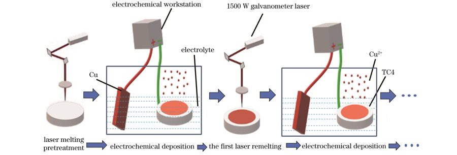
    Fig. 1. Flowchart of laser remelting/electrochemical deposition interaction experiment
    Schematic of electrochemical deposition device
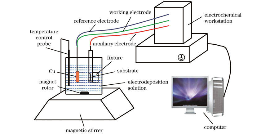
    Fig. 2. Schematic of electrochemical deposition device
    SEM morphologies of surface after laser treatment. (a) After laser melting pretreatment; (b) after laser remelting
    Fig. 3. SEM morphologies of surface after laser treatment. (a) After laser melting pretreatment; (b) after laser remelting
    SEM morphologies of deposited layer surface under laser remelting/electrochemical deposition interaction treatment and conventional electrodeposition process, where the “10” in the figure represents electrodeposition for 10 min and the letter “L” represents laser remelting. (a) Electrodeposition 10 min after laser melting pretreatment; (b) electrodeposition 10 min after the first laser remelting treatment; (c) electrodeposition 10 min after the second laser remelting treatment; (d) conventional electrodeposition for 30 min
    Fig. 4. SEM morphologies of deposited layer surface under laser remelting/electrochemical deposition interaction treatment and conventional electrodeposition process, where the “10” in the figure represents electrodeposition for 10 min and the letter “L” represents laser remelting. (a) Electrodeposition 10 min after laser melting pretreatment; (b) electrodeposition 10 min after the first laser remelting treatment; (c) electrodeposition 10 min after the second laser remelting treatment; (d) conventional electrodeposition for 30 min
    Distribution interval of particle size scale of deposited layer under laser remelting/electrochemical deposition interaction treatment and conventional electrodeposition process. (a) Interactive treatment; (b) conventional electrodeposition
    Fig. 5. Distribution interval of particle size scale of deposited layer under laser remelting/electrochemical deposition interaction treatment and conventional electrodeposition process. (a) Interactive treatment; (b) conventional electrodeposition
    Surface roughness of deposited layer under laser remelting/electrochemical deposition interaction treatment and conventional electrodeposition process. (a) Interactive treatment; (b) conventional electrodeposition
    Fig. 6. Surface roughness of deposited layer under laser remelting/electrochemical deposition interaction treatment and conventional electrodeposition process. (a) Interactive treatment; (b) conventional electrodeposition
    Element distribution of cross-section under laser remelting/electrochemical deposition interaction treatment. (a) Electrodeposition 10 min after laser melting pretreatment; (b) electrodeposition 10 min after the first laser remelting treatment; (c) electrodeposition 10 min after the second laser remelting treatment
    Fig. 7. Element distribution of cross-section under laser remelting/electrochemical deposition interaction treatment. (a) Electrodeposition 10 min after laser melting pretreatment; (b) electrodeposition 10 min after the first laser remelting treatment; (c) electrodeposition 10 min after the second laser remelting treatment
    Section thickness of deposited layer under laser remelting/electrochemical deposition interaction treatment and traditional electrodeposition process. (a) Electrodeposition 10 min after laser melting pretreatment; (b) electrodeposition 10 min after the first laser remelting treatment; (c) electrodeposition 10 min after the second laser remelting treatment; (d) conventional electrodeposition for 30 min
    Fig. 8. Section thickness of deposited layer under laser remelting/electrochemical deposition interaction treatment and traditional electrodeposition process. (a) Electrodeposition 10 min after laser melting pretreatment; (b) electrodeposition 10 min after the first laser remelting treatment; (c) electrodeposition 10 min after the second laser remelting treatment; (d) conventional electrodeposition for 30 min
    XRD phase analysis of composite remelting layer (Ti/Cu composite coating by laser remelting) under laser remelting/electrochemical deposition interaction treatment
    Fig. 9. XRD phase analysis of composite remelting layer (Ti/Cu composite coating by laser remelting) under laser remelting/electrochemical deposition interaction treatment
    Acoustic emission spectra of deposited layer and composite remelting layer under different laser remelting/electrochemical deposition interaction treatment times
    Fig. 10. Acoustic emission spectra of deposited layer and composite remelting layer under different laser remelting/electrochemical deposition interaction treatment times
    SEM morphologies of scratches of deposited layer under laser remelting/electrochemical deposition interaction treatment. (a) Electrodeposition 10 min after laser melting pretreatment; (b) electrodeposition 10 min after the first laser remelting treatment; (c) electrodeposition 10 min after the second laser remelting treatment
    Fig. 11. SEM morphologies of scratches of deposited layer under laser remelting/electrochemical deposition interaction treatment. (a) Electrodeposition 10 min after laser melting pretreatment; (b) electrodeposition 10 min after the first laser remelting treatment; (c) electrodeposition 10 min after the second laser remelting treatment
    SEM morphologies of scratch of composite remelting layer obtained by laser remelting/electrochemical deposition interaction treatment. (a) The first laser remelting treatment after electrodeposition 10 min; (b) the second laser remelting treatment after electrodeposition 20 min; (c) the third laser remelting treatment after electrodeposition 30 min
    Fig. 12. SEM morphologies of scratch of composite remelting layer obtained by laser remelting/electrochemical deposition interaction treatment. (a) The first laser remelting treatment after electrodeposition 10 min; (b) the second laser remelting treatment after electrodeposition 20 min; (c) the third laser remelting treatment after electrodeposition 30 min
    Oxidative weight gain of interaction-deposited samples and conventional electrodeposition samples at 600 ℃
    Fig. 13. Oxidative weight gain of interaction-deposited samples and conventional electrodeposition samples at 600 ℃
    Electrical resistivity of coating samples under laser remelting/electrochemical deposition interaction treatment and conventional electrodeposition process
    Fig. 14. Electrical resistivity of coating samples under laser remelting/electrochemical deposition interaction treatment and conventional electrodeposition process
    Timing potential curves of copper electrodeposition process under laser remelting/electrochemical deposition interaction treatment
    Fig. 15. Timing potential curves of copper electrodeposition process under laser remelting/electrochemical deposition interaction treatment
    Schematic of laser remelting/electrochemical deposition interaction treatment
    Fig. 16. Schematic of laser remelting/electrochemical deposition interaction treatment
    ProcessLight spot diameter /µmPower/WScan speed/(mm·s-1Line spacing/mm
    Laser melting treatment2005003000.05
    Laser remelting2005003000.04
    Table 1. Process parameters of laser melting treatment and laser remelting
    IngredientContent
    Volume of deionized water /mL200
    Mass of CuSO4 /g45
    Volume of H2SO4 /mL13
    Table 2. Composition and content of electrodeposition solution
    SampleCritical load /N
    1044.80
    10-L-1047.15
    10-L-10-L-1049.35
    10-L49.60
    10-L-10-L49.80
    10-L-10-L-10-L49.95
    Table 3. Critical load of deposited layer and composite remelting layer under different laser remelting/ electrochemical deposition interaction treatment times
    Tingchao Xiong, Yanyi Yin, Danhua Lu, Guolong Wu, Ye Wang, Jianhua Yao. Microstructure and Mechanism of Copper Layer Processed with Laser Remelting and Electrochemical Deposition Interaction Process[J]. Chinese Journal of Lasers, 2023, 50(4): 0402007
    Download Citation