
Roel Baets, Bart Kuyken, "High speed phase modulators for silicon photonic integrated circuits: a role for lithium niobate?," Adv. Photon. 1, 030502 (2019)
- Advanced Photonics
- Vol. 1, Issue 3, 030502 (2019)
Abstract
Lithium niobate (LN) has been and still is a prominent material for high speed optical modulators. The performance of such LN-modulators—as a stand-alone building block for optical systems—has been unchallenged for many years. But in many ways it has proven to be very hard to integrate lithium niobate modulators with other functions on a single optical chip. As a result, scientific interest in this material has been fading away. As a consequence of the success in the development of thin film lithium niobate, recent reports
Ever since the seminal paper by Stewart Miller in 1969
For several decades most of the research efforts would focus on the key building blocks: passive optical functions such as spectral filtering, electro-optical modulation, optical amplification, laser emission, light detection, and more. Given the difficulty of achieving all these functions in a single material system, the field diverged. For purely passive functions low loss dielectric materials were chosen, with silica being an important example. The term “planar lightwave circuit” (PLC) was typically used for such passive chips. For light amplification and laser emission III-V semiconductors were the primary material of choice, with the exact material choice dictated by the wavelength of operation. Here one would take advantage of the power of epitaxy to create layer structures that would at the same time provide confinement for free charge carriers (electrons and holes) as well as for photons. For optical phase modulation one would resort to electro-optic materials with a strong Pockels effect. The Pockels effect is an ultra-fast and optically broadband electro-optic effect in which an electric field induces changes to the relative position of bound electrons and atomic nuclei, which translates into a refractive index change that scales linearly with the applied electric field. This allows for pure phase modulators. The Pockels effect can only occur in materials that lack inversion symmetry, such as in non-centro-symmetric crystals (like LN) or poled polymers.
Sign up for Advanced Photonics TOC. Get the latest issue of Advanced Photonics delivered right to you!Sign up now
LN has been the most successful material for high speed optical modulation, due to its strong Pockels effect, first as a bulk material and later in the form of planar waveguide-based components. While the basic modulation effect is based on index modulation, and therefore optical phase modulation, it is relatively straightforward to convert that into amplitude modulation, either by combining the modulator with polarizers or by making use of an interferometric construct in which one path is phase modulated and another path is not or inversely modulated. Upon recombination of both paths amplitude modulation results. The key performance metric of such a modulator is the voltage
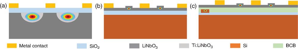
The status quo as described above has been broken recently through the use of high-index-contrast photonics. Indeed, the waveguides described earlier were typically low-index-contrast waveguides in which in-diffused ions provided the (very weak) index contrast between core and cladding, with a weak optical confinement as a result (
![]()
Figure 1.(a) A traditional lithium niobate modulator; (b) a cross-section of the modulator of Ref.
However impressive the performance of this result is, the LN-modulator is still a discrete component. In the past few decades the field of photonic integration has been moving in the direction of platforms that enable the integration of photonic circuits with a diversity of passive and active components within one circuit. This is a non-trivial task because different materials are good at different functionalities. Therefore integrating multiple functionalities within one materials platform typically leads to compromises on performance, at least in an early phase. Nevertheless the benefits in terms of cost and reliability resulting from the integration on one platform are important enough to make it highly relevant from an industrial point of view. Moreover, when many research and industrial actors focus their efforts on one platform, a virtuous circle arises in which advancement of performance accelerates and economy-of-scale effects create an ecosystem in which fabs and fabless users can thrive.
While the notion of a one-platform-approach has been tried with multiple materials, it is quite clear by now that silicon photonics is gaining the largest momentum. Silicon photonics makes use of the tool sets and process flows found in CMOS fabs to manufacture photonic integrated circuits with silicon of silicon-nitride-based waveguides, interconnecting a diversity of components. The most common modality is to use silicon-on-insulator (SOI) wafers in which passive silicon waveguides are formed along with waveguides with p-n junctions to form phase modulators, based on the modulation of the free carrier concentration, as well as monolithic germanium detectors. With this combination a variety of impressive products has been developed, in particular high symbol rate (at least up to 40 Gbaud) optical transceivers for the telecom and datacom market.
Silicon and germanium do lack the proper material characteristics however for all functionalities that one may wish for. Not only is light emission highly inefficient, also the Pockels effect is absent. Therefore it is not possible to build a pure phase modulator in a similar way as is the case in LN. While the free-carrier-based modulators mentioned earlier perform quite well, they have intrinsic limitations in speed and optical loss. Moreover, they do not allow for pure phase modulation because there is residual amplitude modulation due to free carrier induced loss. Already today they are used more or less at a performance level close to physical limits, but the market is calling for even higher performance so as to address the insatiable demands for bandwidth. This is where heterogeneous integration comes in, whereby a diversity of materials is co-integrated on a silicon photonics platform. In the case of amorphous materials the co-integration can be done by straightforward thin film deposition (sputtering, plasma-enhanced deposition, atomic layer deposition, etc.), but in the case of crystalline materials one needs to resort to more sophisticated methods. One may try to use an epitaxial growth technique directly on silicon (or a deposition technique followed by anneal to create a crystalline phase), but this is typically very demanding and only possible for certain material combinations. Invariably it also involves a process step at elevated temperatures. The alternative is to start from a crystalline thin film grown onto a different host substrate and then somehow transfer and bond that film to the silicon photonics wafer. Methods to do so have become relatively mature in recent years. Either they use bonding of the thin film to the silicon wafer with subsequent removal of the host substrate
In Ref.
These results show the potential of how miniaturization enabled by high index contrast can enhance the performance of devices. By using the high confinement in thin film layers very efficient modulators result. Moreover, by relying on a heterogeneous integration technique, Ref.


Set citation alerts for the article
Please enter your email address

© Copyright 2018-2021 | Chinese Laser Press. All Rights Reserved 沪ICP备15018463号-20