
Junting Liu, He Yang, Vladislav Khayrudinov, Harri Lipsanen, Hongkun Nie, Kejian Yang, Baitao Zhang, Jingliang He, "Ultrafast carrier dynamics and nonlinear optical response of InAsP nanowires," Photonics Res. 9, 1811 (2021)
- Photonics Research
- Vol. 9, Issue 9, 1811 (2021)
Abstract
1. INTRODUCTION
In the past two decades, nanowires (NWs) have been employed as versatile building blocks [1–3] used in various optoelectrical devices [4–7] because of their tailored optical and electronic properties [8,9]. Semiconductor NWs exhibit many unique physical characteristics such as significant surface and size effects [10], building blocks for nanoelectronics [7], and Majorana fermions [11]. For example, the electrical and optical properties of semiconductor NWs can be tuned by controlling their sizes, shapes, and compositions [12,13]. For instance, alloyed III–V semiconductor ternary
Owing to the large electron g-factor and small electron effective mass [17–19], III–V semiconductor NWs have been applied in nanoscale optoelectronic devices [17], infrared detectors [18], and spin electronics [19]. Known as the representative of the III–V semiconductor family, InAsP NWs which were first synthesized by Pettersson in 2006 [3] show great potential for infrared photodetectors due to the high carrier mobility. Since then, great efforts have been devoted to pursuing InAsP NW-based optoelectronic devices, such as high-speed electronics [20,21] and near-infrared light emitters and detectors [22–24]. In theory, the bandgap of InAsP NWs can be tailored from 0.35 to 1.35 eV by adjusting the alloy composition, covering the important telecommunication wavelength band from 1.3 to 1.55 μm [25]. Besides, the growth of InAsP NWs has larger tolerance for lattice mismatch than thin-film epitaxial growth, which allows adjusting the optical nonlinear sensitivity through external bending or twisting strain [26,27] and has more flexibility in substrate selection and mechanical properties. Thus, there is a demand to study the intrinsic optical properties (e.g., carrier dynamics, nonlinear optical absorption) of InAsP NWs in the near-infrared wavelength range, which remains unexplored.
In this work, we fabricate high-quality InAsP NWs by directly growing them on a quartz substrate using the Au nanoparticle-assisted vapor-liquid-solid (VLS) method. Then, the carrier dynamics of InAsP NWs is investigated by nondegenerate pump-probe measurements, which show that the excited carrier in InAsP NWs exhibits one fast (
Sign up for Photonics Research TOC. Get the latest issue of Photonics Research delivered right to you!Sign up now
2. RESULTS AND DISCUSSION
A. Preparation and Characterization of InAsP NWs
InAsP NWs samples are grown on quartz substrates inside a horizontal flow atmospheric pressure metal-organic vapor phase epitaxy (MOVPE) system. The detailed process can be found in Appendix A.1. Scanning electron microscopy (SEM) is used to examine the surface morphology of the prepared NWs. Figure 1(a) depicts the as-grown InAsP NWs that have an average diameter of
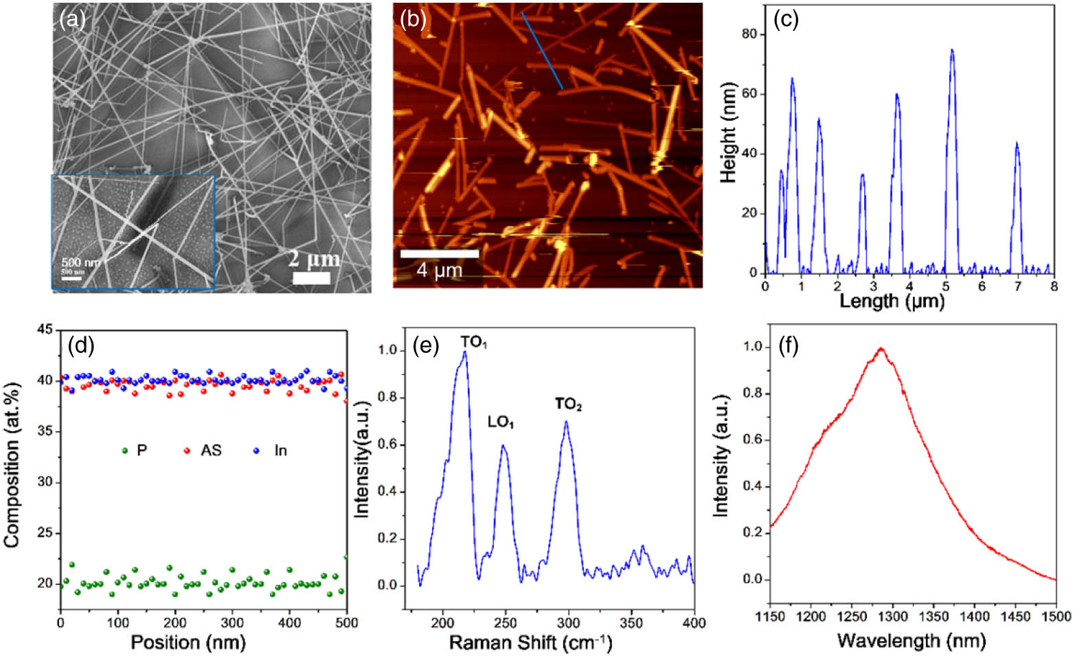
Figure 1.(a) SEM image of InAsP NWs on quartz substrate. The inset is a higher-resolution SEM image, which shows the NW diameter of
B. Ultrafast Carrier Dynamics of InAsP NWs
![]()
Figure 2.(a) Experimental setup of the nondegenerate pump-probe measurement. (b) Differential transmission of InAsP NWs at different pump pulse energies with a 675 nm probe laser. (c) Relationship between maximum differential transmission and initial photoinduced carrier density. (d) Linear fit to
The photoinduced carrier dynamics relaxed from the excited states to the valence band is commonly described by a three-term rate equation [32–34]:
After converting the measured
C. Nonlinear Optical Response of InAsP NWs
![]()
Figure 3.Characterization of the NLO properties of the InAsP NWs. OA Z-scan measurements of the InAsP NWs at (a) 532 nm and (c) 1064 nm. CA Z-scan measurements of the InAsP NWs at (b) 532 nm and (d) 1064 nm.
The CA Z-scan technique is used to characterize the refractive index (
D. Ultrafast Photonic Applications
Because InAsP NWs exhibit strong third-order nonlinear optical response and ultrafast saturation recovery time, it is meaningful to further explore their ability on the generation of ultrashort pulses. Here, a mode-locked solid-state laser based on InAsP NWs saturable absorber is assembled. Based on the mode-locking theory, when the mode-locking pulse energy is larger than the minimum intracavity pulse energy, the stable continuous-wave (CW) laser can be demonstrated. Therefore, considering the SA parameters, the following formula should be satisfied [41]:
When the absorbed pump power exceeds 4.26 W, stable CW mode-locked (CWML) operation is established. Figure 4(a) depicts the relationship between the absorbed pump power and average output power. The obtained maximum average output power is 333 mW under the absorbed pump power of 7.17 W. Once the absorbed pump power exceeds 7.17 W, the CWML operation is broken. The output power instabilities (RMS) are measured to be less than 2% over 1 h. By
![]()
Figure 4.Mode-locked laser results based on InAsP NWs. (a) Average output power versus absorbed pump power. (b) The measured pulse width by autocorrelation spectroscopy is
3. CONCLUSIONS
In summary, we fabricate InAsP NWs by using an Au nanoparticle-assisted VLS growth method. The NLO properties and ultrafast carrier dynamics of InAsP NWs have been studied by Z-scan and nondegenerate pump-probe measurements for the first time. The excited carriers of InAsP NWs exhibit two characteristic carrier lifetimes (fast
Acknowledgment
Acknowledgment. H.Y. acknowledges the support from EU. V.K. acknowledges the support of Aalto University Doctoral School, Walter Ahlström Foundation, Elektroniikkainsinöörien Säätiö, Sähköinsinööriliiton Säätiö, and Nokia Foundation Finnish Foundation for Technology Promotion (Tekniikan Edistämissäätiö) and Waldemar Von Frenckells foundation. H.L. and V.K. acknowledge support from the Academy of Finland Flagship Programme, Photonics Research and Innovation (PREIN), decision number: 320167. V.K. and H.Y. acknowledge the provision of facilities and technical support by Aalto University at Micronova Nanofabrication Centre.
APPENDIX A: EXPERIMENTAL METHODS
InAsP NWs were grown on quartz substrates inside a horizontal flow atmospheric pressure metal-organic vapor phase epitaxy (MOVPE) system using an Au nanoparticle–assisted vapor-liquid-solid (VLS) growth method. Trimethylindium (TMIn), tertiarybutylarsene (TBAs) and tertiarybutylphosphine (TBP) were used as precursors. First, the substrates were cleaned in an ultrasonic bath with isopropanol (IPA) and acetone, rinsed in deionized water, and then treated with a poly-L-lysine (PLL) solution for 120 s. Next, the surface was treated with 40 nm diameter colloidal gold (Au) nanoparticles solution (BBI International, UK) for 120 s. Prior to the growth, the substrates were annealed in situ at 600°C for 10 min under hydrogen flow to desorb surface contaminants. The NW growth temperature was fixed at 410°C for 5 min with the TMIn, TBAs, and TBP flows of 2.8, 14.4, and 1276 μmol/min, respectively. The nominal V/III ratio during the growth was
The setup was established using Ti:sapphire oscillators (800 nm, 80 MHz, 150 fs), separated to two components. One beam was used to drive the optical parametric oscillator to generate the pulses from 1000 to 1500 nm. After frequency doubling through a BBO crystal, the wavelength of the beam was changed to 500–750 nm. The wavelength of 650 nm was used as the probe light. The other beam was fixed at 400 nm and was used as the pump light. Both the pump and probe light were focused onto the sample by a
Z-scan measurements were performed using a homemade mode-locked Yb fiber laser (center wavelength 1064 nm, repetition rate 100 kHz–1 MHz, pulse duration 10 ps), which can generate a signal with the wavelength of 532 nm by doubling the frequency through a BBO crystal. The pulses were divided to two parts: one was set as a reference light, collected by a power meter (Thorlabs S470C); the other was focused by a lens into the samples. Lenses of different focusing lengths were used for different wavelength of incident light,
We transferred the as-grown InAsP NWs grown on quartz onto a mirror with high-reflection (HR) coating at 1020–1100 nm via a PMMA-mediated method.
APPENDIX B: THE FITTING PARAMETERS OBTAINED FROM Z-SCAN CHARACTERIZATION
As shown in Table
Fitting Parameters Obtained from Z-Scan Characterization of InAsP NWs under Different Excitation Energies
| Wavelength | Input | ||||||
|---|---|---|---|---|---|---|---|
| 532 | 0.25 | ||||||
| 0.16 | |||||||
| 0.055 | |||||||
| 1064 | 1.01 | ||||||
| 0.55 | |||||||
| 0.33 |
APPENDIX C: THE NONLINEAR TRANSMITTANCE CURVE OF InAsP NWS
As shown in Fig.
![]()
Figure 5.(a)–(c) Nonlinear transmittance of the InAsP NWs at the wavelength of 532 nm with different incident pulse energies. (d)–(f) Nonlinear transmittance of the InAsP NWs at the wavelength of 1064 nm with different incident pulse energies.
APPENDIX D: THE EXPERIMENTAL SETUP OF THE MODE-LOCKED SOLID-STATE LASER
In our experiment, a z-type resonator with the cavity length of 3.49 m is applied, as shown in Fig.
![]()
Figure 6.Experimental setup of the mode-locked solid-state bulk laser based on an InAsP NWs SA.
References
[1] J. Wallentin, N. Anttu, D. Asoli, M. Huffman, I. Åberg, M. H. Magnusson, G. Siefer, P. Fuss-Kailuweit, F. Dimroth, B. Witzigmann, H. Q. Xu, L. Samuelson, K. Deppert, M. T. Borgström. InP nanowire array solar cells achieving 13.8% efficiency by exceeding the ray optics limit. Science, 339, 1057-1060(2013).
[2] H. Zhu, Y. Fu, F. Meng, X. Wu, Z. Gong, Q. Ding, M. V. Gustafsson, M. T. Trinh, S. Jin, X. Y. Zhu. Lead halide perovskite nanowire lasers with low lasing thresholds and high quality factors. Nat. Mater., 14, 636-642(2015).
[3] H. Pettersson, J. Trägårdh, A. I. Persson, L. Landin, D. Hessman, L. Samuelson. Infrared photodetectors in heterostructure nanowires. Nano Lett., 6, 229-232(2006).
[4] N. Engheta. Circuits with light at nanoscales: optical nanocircuits inspired by metamaterials. Science, 317, 1698-1702(2007).
[5] Y. S. No, L. Xu, M. N. Mankin, H. G. Park. Shape-controlled assembly of nanowires for photonic elements. ACS Photon., 3, 2285-2290(2016).
[6] J. Kim, H. C. Lee, K. H. Kim, M. S. Hwang, J. S. Park, J. M. Lee, J. P. So, J. H. Choi, S. H. Kwon, C. J. Barrelet, H. G. Park. Photon-triggered nanowire transistors. Nat. Nanotechnol., 12, 963-968(2017).
[7] Y. Cui, C. M. Lieber. Functional nanoscale electronic devices assembled using silicon nanowire building blocks. Science, 291, 851-853(2001).
[8] D. M. Lyons, K. M. Ryan, M. A. Morris, J. D. Holmes. Tailoring the optical properties of silicon nanowire arrays through strain. Nano Lett., 2, 811-816(2002).
[9] L. B. Luo, F. X. Liang, X. L. Huang, T. X. Yan, J. G. Hu, Y. Q. Yu, C. Y. Wu, L. Wang, Z. F. Zhu, Q. Li, J. S. Jie. Tailoring the electrical properties of tellurium nanowires via surface charge transfer doping. J. Nanopart. Res., 14, 967-976(2012).
[10] S. M. Bergin, Y. H. Chen, B. J. Wiley. The effect of nanowire length and diameter on the properties of transparent, conducting nanowire films. Nanoscale, 4, 1996-2004(2012).
[11] V. Mourik, K. Zuo, S. M. Frolov, S. R. Plissard, E. Bakkers, L. P. Kouwenhoven. Signatures of majorana fermions in hybrid superconductor-semiconductor nanowire devices. Science, 336, 1003-1007(2012).
[12] L. Balaghi, G. Bussone, J. Grenzer, M. Ghorbani, A. Krasheninnikov, H. Schneider. Widely tunable GaAs bandgap via strain engineering in core/shell nanowires with large lattice mismatch. Nat. Commun., 10, 2793(2019).
[13] M. Li, J. C. Li. Size effects on the band-gap of semiconductor compounds. Mater. Lett., 60, 2526-2529(2006).
[14] I. Åberg, G. Vescovi, D. Asoli, U. Naseem, J. P. Gilboy, C. Sundvall, A. Dahlgren, K. E. Svensson, N. Anttu, M. T. Björk, L. Samuelson. A GaAs nanowire array solar cell with 15.3% efficiency. IEEE J. Photovolt., 6, 185-190(2016).
[15] Z. Liu, L. Yin, H. Ning, Z. Yang, L. Tong, C. Z. Ning. Dynamical color-controllable lasing with extremely wide tuning range from red to green in a single alloy nanowire using nanoscale manipulation. Nano Lett., 13, 4945-4950(2013).
[16] M. D. Thompson, A. Alhodaib, A. P. Craig, A. Robson, A. Aziz, A. Krier, J. Svensson, L. E. Wernersson, A. M. Sanchez, A. R. Marshall. Low leakage-current InAsSb nanowire photodetectors on silicon. Nano Lett., 16, 182-187(2016).
[17] A. L. Efros, M. Rosen. The electronic structure of semiconductor nanocrystals. Annu. Rev. Mater. Res., 30, 475-521(2000).
[18] S. K. Lim, M. Brewster, F. Qian, Y. Li, C. M. Lieber, S. Gradečak. Direct correlation between structural and optical properties of III−V nitride nanowire heterostructures with nanoscale resolution. Nano Lett., 9, 3940-3944(2009).
[19] J. Hou, B. Zhang, X. Su, R. Zhao, Z. Wang, F. Lou, J. He. High efficient mode-locked Tm:YAP laser emitting at 1938 nm by SESAM. Opt. Commun., 347, 88-91(2015).
[20] J. H. Lee, M. W. Pin, S. J. Choi, M. H. Jo, J. C. Shin, S. G. Hong, S. M. Lee, B. Cho, S. J. Ahn, N. W. Song, S. H. Yi, Y. H. Kim. Electromechanical properties and spontaneous response of the current in InAsP nanowires. Nano Lett., 16, 6738-6745(2016).
[21] E. Lind, A. I. Persson, L. Samuelson, L. E. Wernersson. Improved subthreshold slope in an InAs nanowire heterostructure field-effect transistor. Nano Lett., 6, 1842-1846(2006).
[22] M. Takiguchi, N. Takemura, K. Tateno, K. Nozaki, S. Sasaki, S. Sergent, E. Kuramochi, T. Wasawo, A. Yokoo, A. Shinya, M. Notomi. All-optical InAsP/InP nanowire switches integrated in a Si photonic crystal. ACS Photon., 7, 1016-1021(2020).
[23] M. Karimi, M. Heurlin, S. Limpert, V. Jain, X. Zeng, I. Geijselaers, A. Nowzari, Y. Fu, L. Samuelson, H. Linke, M. T. Borgstrom, H. Pettersson. Intersubband quantum disc-in-nanowire photodetectors with normal-incidence response in the long-wavelength infrared. Nano Lett., 18, 365-372(2018).
[24] J. Treu, M. Bormann, H. Schmeiduch, M. Doblinger, S. Morkotter, S. Matich, P. Wiecha, K. Saller, B. Mayer, M. Bichler, M. C. Amann, J. J. Finley, G. Abstreiter, G. Koblmuller. Enhanced luminescence properties of InAs-InAsP core-shell nanowires. Nano Lett., 13, 6070-6077(2013).
[25] Q. Hu, P. Li, B. Zhang, B. Liu, L. Wang, X. Chen. Passively
[26] X. Han, K. Wang, H. Long, H. Hu, J. Chen, B. Wang, P. Lu. Highly sensitive detection of the lattice distortion in single bent ZnO nanowires by second-harmonic generation microscopy. ACS Photon., 3, 1308-1314(2016).
[27] N. M. Jassim, K. Wang, X. Han, H. Long, B. Wang, P. Lu. Plasmon assisted enhanced second-harmonic generation in single hybrid Au/ZnS nanowires. Opt. Mater., 64, 257-261(2017).
[28] R. Carles, N. Saint-Cricq, J. B. Renucci, R. J. Nicholas. Raman scattering in InP1-
[29] J. Guo, R. Shi, R. Wang, Y. Wang, F. Zhang, C. Wang, H. Chen, C. Ma, Z. Wang, Y. Ge, Y. Song, Z. Luo, D. Fan, X. Jiang, J. Xu, H. Zhang. Graphdiyne-polymer nanocomposite as a broadband and robust saturable absorber for ultrafast photonics. Laser Photon. Rev., 14, 1900367(2020).
[30] M. Breusing, C. Ropers, T. Elsaesser. Ultrafast carrier dynamics in graphite. Phys. Rev. Lett., 102, 086809(2009).
[31] H. Wang, C. Zhang, F. Rana. Surface recombination limited lifetimes of photoexcited carriers in few-layer transition metal dichalcogenide MoS2. Nano Lett., 15, 8204-8210(2015).
[32] D. Sun, Y. Rao, G. A. Reider, G. Chen, Y. You, L. Brezin, A. R. Harutyunyan, T. F. Heinz. Observation of rapid exciton-exciton annihilation in monolayer molybdenum disulfide. Nano Lett., 14, 5625-5629(2014).
[33] J. S. Manser, P. V. Kamat. Band filling with free charge carriers in organometal halide perovskites. Nat. Photonics, 8, 737-743(2014).
[34] M. Ghanassi, M. C. Schanne-Klein, F. Hache, A. I. Ekimov, D. Ricard, C. Flytzanis. Time-resolved measurements of carrier recombination in experimental semiconductor-doped glasses: confirmation of the role of Auger recombination. Appl. Phys. Lett., 62, 78-80(1993).
[35] I. Robel, B. A. Bunker, P. V. Kamat, M. Kuno. Exciton recombination dynamics in CdSe nanowires: bimolecular to three-carrier Auger kinetics. Nano Lett., 6, 1344-1349(2006).
[36] V. I. Klimov, A. A. Mikhailovsky, D. W. McBranch, C. A. Leatherdale, M. G. Bawendi. Quantization of multiparticle Auger rates in semiconductor quantum dots. Science, 287, 1011-1013(2000).
[37] J. Guo, D. Huang, Y. Zhang, H. Yao, Y. Wang, F. Zhang, R. Wang, Y. Ge, Y. Song, Z. Guo, F. Yang, J. Liu, C. Xing, T. Zhai, D. Fan, H. Zhang. 2D GeP as a novel broadband nonlinear optical material for ultrafast photonics. Laser Photon. Rev., 13, 1900123(2019).
[38] K. Wang, Y. Feng, C. Chang, J. Zhan, C. Wang, Q. Zhao, J. N. Coleman, L. Zhang, W. J. Blau, J. Wang. Broadband ultrafast nonlinear absorption and nonlinear refraction of layered molybdenum dichalcogenide semiconductors. Nanoscale, 6, 10530-10535(2014).
[39] S. Bikorimana, P. Lama, A. Walser, R. Dorsinville, S. Anghel, A. Mitioglu, A. Micu, L. Kulyuk. Nonlinear optical responses in two-dimensional transition metal dichalcogenide multilayer: WS2, WSe2, MoS2 and Mo0.5W0.5S2. Opt. Express, 24, 20685-20695(2016).
[40] K. Wang, B. M. Szydlowska, G. Wang, X. Zhang, J. J. Wang, J. J. Magan, L. Zhang, J. N. Coleman, J. Wang, W. J. Blau. Ultrafast nonlinear excitation dynamics of black phosphorus nanosheets from visible to mid-infrared. ACS Nano, 10, 6923-6932(2016).
[41] X. Jiang, S. Liu, W. Liang, S. Luo, Z. He, Y. Ge, H. Wang, R. Cao, F. Zhang, Q. Wen, J. Li, Q. Bao, D. Fan, H. Zhang. Broadband nonlinear photonics in few-layer MXene Ti3C2T
[42] J. Liu, V. Khayrudinov, H. Yang, Y. Sun, B. Matveev, M. Remennyi, K. Yang, T. Haggren, H. Lipsanen, F. Wang, B. Zhang, J. He. InAs-nanowire-based broadband ultrafast optical switch. J. Phys. Chem. Lett., 10, 4429-4436(2019).
[43] M. Sheik-Bahae, A. A. Said, T. Wei, D. J. Hagan, E. W. V. Stryland. Sensitive measurement of optical nonlinearities using a single beam. IEEE J. Quantum Electron., 26, 760-769(1990).


Set citation alerts for the article
Please enter your email address

© Copyright 2018-2021 | Chinese Laser Press. All Rights Reserved 沪ICP备15018463号-20