• Chinese Physics B
  • Vol. 29, Issue 9, (2020)
Shuya Xing1, Le Lei1, Haoyu Dong1, Jianfeng Guo1, Feiyue Cao1, Shangzhi Gu1, Sabir Hussain2、3, Fei Pang1、†, Wei Ji1, Rui Xu1, and Zhihai Cheng1
Author Affiliations
  • 1Beijing Key Laboratory of Optoelectronic Functional Materials & Micro-nano Devices, Department of Physics, Renmin University of China, Beijing 00872, China
  • 2CAS Key Laboratory of Standardization and Measurement for Nanotechnology, CAS Center for Excellence in Nanoscience, National Center for Nanoscience and Technology, Beijing 100190, China
  • 3University of Chinese Academy of Sciences, Beijing 10009, China
  • show less
    DOI: 10.1088/1674-1056/aba27c Cite this Article
    Shuya Xing, Le Lei, Haoyu Dong, Jianfeng Guo, Feiyue Cao, Shangzhi Gu, Sabir Hussain, Fei Pang, Wei Ji, Rui Xu, Zhihai Cheng. Epitaxial growth of antimony nanofilms on HOPG and thermal desorption to control the film thickness[J]. Chinese Physics B, 2020, 29(9): Copy Citation Text show less
    Atomic structural models of antimonene allotropes. (a) Top view and side view of α-Sb. (b) Top view and side view of β-Sb.
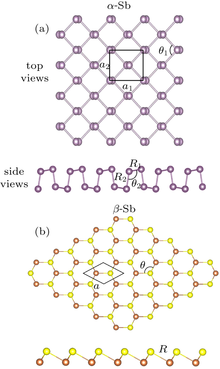
    Fig. 1. Atomic structural models of antimonene allotropes. (a) Top view and side view of α-Sb. (b) Top view and side view of β-Sb.
    Epitaxial growth of the Sb nanofilms on HOPG substrates at various temperatures. The HOPG substrate was kept at 304 K (a)–(c), 314 K (d)–(f), 355 K (g)–(i), and 371 K (j)–(l) respectively during growth. (a), (d), (g), (j) Large-scale SEM images show the general morphology of Sb nanofilms. (b), (e), (g), (k) The zoom in SEM images show more structural details of Sb nanofilms. (c), (f), (i), (l) AFM topography images show the thickness of Sb nanofilms.
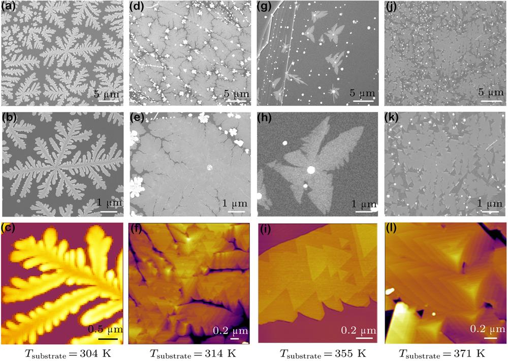
    Fig. 2. Epitaxial growth of the Sb nanofilms on HOPG substrates at various temperatures. The HOPG substrate was kept at 304 K (a)–(c), 314 K (d)–(f), 355 K (g)–(i), and 371 K (j)–(l) respectively during growth. (a), (d), (g), (j) Large-scale SEM images show the general morphology of Sb nanofilms. (b), (e), (g), (k) The zoom in SEM images show more structural details of Sb nanofilms. (c), (f), (i), (l) AFM topography images show the thickness of Sb nanofilms.
    STM measurements of the β-Sb nanofilm on HOPG. (a) Schematic of the deposition process. (b) STM topographic image (Vt = 2.1 V, It = 400 pA) of the Sb nanofilm with the edges. (c) The height line profiles show the thickness (purple) and single step height (red) of the Sb nanofilm, respectively. (d) RHEED pattern of the Sb nanofilm on HOPG. (e) Atomic resolution STM image (Vt = –1.4 V, It = 700 pA) of Sb nanofilm with the overlaid atomic structural model. Inset: line profile along the blue line, showing the periodicity of β-Sb lattice (4.2 Å). (f) STM image of the Moiré pattern was occasionally observed (Vt = 2.4 V, It = 300 pA) in Sb nanofilms. The insert line profile presents the period and amplitude of the Moiré pattern. (g) Atomic resolution image of (f) (Vt = 2.4 V, It = 300 pA,). (h) Schematic structural model of (g). The high symmetric sites are marked by the corresponding color circles in (h) and dots in (g): TOP (red), HCP (purple), BRIDGE (green), and FCC (blue). (i) FFT of the atomic resolution image of (g).
    Fig. 3. STM measurements of the β-Sb nanofilm on HOPG. (a) Schematic of the deposition process. (b) STM topographic image (Vt = 2.1 V, It = 400 pA) of the Sb nanofilm with the edges. (c) The height line profiles show the thickness (purple) and single step height (red) of the Sb nanofilm, respectively. (d) RHEED pattern of the Sb nanofilm on HOPG. (e) Atomic resolution STM image (Vt = –1.4 V, It = 700 pA) of Sb nanofilm with the overlaid atomic structural model. Inset: line profile along the blue line, showing the periodicity of β-Sb lattice (4.2 Å). (f) STM image of the Moiré pattern was occasionally observed (Vt = 2.4 V, It = 300 pA) in Sb nanofilms. The insert line profile presents the period and amplitude of the Moiré pattern. (g) Atomic resolution image of (f) (Vt = 2.4 V, It = 300 pA,). (h) Schematic structural model of (g). The high symmetric sites are marked by the corresponding color circles in (h) and dots in (g): TOP (red), HCP (purple), BRIDGE (green), and FCC (blue). (i) FFT of the atomic resolution image of (g).
    Thermal desorption to control the thickness of Sb nanofilms. (a) and (b) SEM image and AFM image of the Sb nanofilm before desorption, respectively. (c) and (d) SEM image and AFM image of the Sb nanofilm after desorption, respectively. The height line profile shows the thickness of the desorbed Sb nanofilms at ∼ 3.27 nm. (e) Large-scale STM topographic image of Sb nanofilm after thermal desorption. The Sb nanofilm has been partially desorbed (Vt = 2.14 V, It = 300 pA). (f) During the desorption, the Sb atoms can redeposit to form small triangular islands (Vt = –2.4 V, It = 150 pA). STM images (g) and (h) reveal that many triangular holes are formed on the surface of the desorbed Sb nanofilm (Vt = 2.0 V, It = 100 pA). (i) Atomic resolution at step edge of the triangular hole. The atomic structural model of β-Sb is superimposed on the step edge (Vt = 0.1 V, It = 800 pA).
    Fig. 4. Thermal desorption to control the thickness of Sb nanofilms. (a) and (b) SEM image and AFM image of the Sb nanofilm before desorption, respectively. (c) and (d) SEM image and AFM image of the Sb nanofilm after desorption, respectively. The height line profile shows the thickness of the desorbed Sb nanofilms at ∼ 3.27 nm. (e) Large-scale STM topographic image of Sb nanofilm after thermal desorption. The Sb nanofilm has been partially desorbed (Vt = 2.14 V, It = 300 pA). (f) During the desorption, the Sb atoms can redeposit to form small triangular islands (Vt = –2.4 V, It = 150 pA). STM images (g) and (h) reveal that many triangular holes are formed on the surface of the desorbed Sb nanofilm (Vt = 2.0 V, It = 100 pA). (i) Atomic resolution at step edge of the triangular hole. The atomic structural model of β-Sb is superimposed on the step edge (Vt = 0.1 V, It = 800 pA).
    Strained Moiré superstructures of the Sb nanofilms after thermal desorption. (a) and (b) STM images of Moiré pattern by the thermal strain during the desorption (Vt = 2.4 V, It = 200 pA). The grain boundaries (GBs) separate the strained Moiré area and unstrained flat area of Sb nanofilms. (c) The magnified image at the grain step edge. (d) Atomic resolution image of the dislocation (Vt = 0.2 V, It = 400 pA). (e) FFT of the atomic resolution image of (d). (f) Schematic model of the dislocation of a 4° GB. (D = b/θ, and θ=tan−1(1/(3(2n+1))), n = 8 here).
    Fig. 5. Strained Moiré superstructures of the Sb nanofilms after thermal desorption. (a) and (b) STM images of Moiré pattern by the thermal strain during the desorption (Vt = 2.4 V, It = 200 pA). The grain boundaries (GBs) separate the strained Moiré area and unstrained flat area of Sb nanofilms. (c) The magnified image at the grain step edge. (d) Atomic resolution image of the dislocation (Vt = 0.2 V, It = 400 pA). (e) FFT of the atomic resolution image of (d). (f) Schematic model of the dislocation of a 4° GB. (D = b/θ, and θ=tan1(1/(3(2n+1))), n = 8 here).
    Interfacial interactions and surface potential of the epitaxial Sb nanofilm on HOPG substrate. (a) Schematic diagram of Sb nanofilms manipulated by AFM tip in contact mode. (b) AFM image of the Sb nanofilm on HOPG. After the manipulation, the part of the Sb nanofilm was broken and moved on HOPG surface, as shown in the following AFM image of (c). (d) The corresponding surface potential image of (b) obtained by KPFM measurement. (e) The surface potential difference between Sb nanofilm and HOPG substrate is ∼ 120 mV, as shown in the line profile in (d).
    Fig. 6. Interfacial interactions and surface potential of the epitaxial Sb nanofilm on HOPG substrate. (a) Schematic diagram of Sb nanofilms manipulated by AFM tip in contact mode. (b) AFM image of the Sb nanofilm on HOPG. After the manipulation, the part of the Sb nanofilm was broken and moved on HOPG surface, as shown in the following AFM image of (c). (d) The corresponding surface potential image of (b) obtained by KPFM measurement. (e) The surface potential difference between Sb nanofilm and HOPG substrate is ∼ 120 mV, as shown in the line profile in (d).
    Shuya Xing, Le Lei, Haoyu Dong, Jianfeng Guo, Feiyue Cao, Shangzhi Gu, Sabir Hussain, Fei Pang, Wei Ji, Rui Xu, Zhihai Cheng. Epitaxial growth of antimony nanofilms on HOPG and thermal desorption to control the film thickness[J]. Chinese Physics B, 2020, 29(9):
    Download Citation